- Классификация нано-объектов

Содержание
- 2. Учебный план. Часть 1 – механика нано-объектов в среде Механизмы формирование наносистем в твердых телах. Упругие
- 3. Учебный план. Часть 2 – нано-электро-механические системы Материалы и технология изготовления нано-электро-механических систем. Элементы нано-электро-механических систем.
- 4. Литература Основная Cleland A.N. “Foundations of Nanomechanics” (Springer-Verlag, Berlin, Heidelberg, New York, 2003). Freund L.B., Suresh
- 5. Классификация нано-объектов пленка или слой нить или проволока островок или точка 1D 2D 0D
- 6. Пример: вертикально излучающий лазер vertical cavity surface emitting laser (VCSEL) (a) Schematic of the vertical cavity
- 7. Пример: нано-электро-механические системы (НЭМС) Electron micrographs of silicon NEMS structures made by surface micromachining and e-beam
- 8. Формирование наноструктур Эпитаксия, наращивание, напыление Само-организация на поверхности или в объеме Литография и травление
- 9. Планарные технологии
- 10. Напыление – Sputtering, Physical deposition
- 11. Напыление Бомбардировка ионами, возможно в присутствии внешних полей: СВЧ, магнетронное, и др. Распыляемая мишень осаждается на
- 12. Молекулярно-пучковая (лучевая) эпитаксия – molecular-beam epitaxy (MBE) Схема типичной промышленной установки
- 13. Процессы на поверхности при МПЭ
- 14. Газофазная эпитаксия (Vapor Phase Epitaxy) в хлоридной системе или с использованием металло-органических соединений metal-organic chemical vapor
- 15. Процессы на поверхности при MOCVD Процессы, происходящие при MOCVD
- 16. Моды эпитаксиального роста Технология молекулярно-лучевой эпитаксии (MBE) или газофазной эпитаксии с использованием металлоорганических соединений (MOVPE, MOCVD).
- 17. Движущая сила эпитаксии – пересыщение (supersaturation) газовой фазы и адсорбционного слоя ΔF = kTv ln(p/pe), where
- 18. Само-организация
- 19. Три стадии формирования наночастиц Нуклеация (Nucleation) - Гомогенное или гетерогенное образование зародышей новой фазы за счет
- 20. Поверхностная энергия γ > 0 – коэффициент поверхностного натяжения S – площадь поверхности Формирование частицы новой
- 21. Нуклеация в объеме Работа, необходимая для создания зародыша новой фазы Критический зародыш Вероятность образования зародыша новой
- 22. Нуклеация островка на поверхности Young 1805 θ > 0 – распад пленки на островки (Volmer -
- 23. Нуклеация при пересыщении на поверхности
- 24. Давление под искривленной поверхностью Для двух фаз, находящихся в равновесии, γ = 1 Дж/м2 k =
- 25. Самоорганизация при пересыщении на поверхности Выращивание субмонослойных островков Распад тонких пленок на островки Выращивание усов (whiskers,
- 26. Механизм роста ПЖК Пересыщенный пар кристаллическая подложка пересыщенная жидкость кристалл ус whisker nanowire nanorod
- 27. ZnO nanowires on sapphire (a) Plan view and (b) glancing view of ZnO nanowires grown on
- 28. ZnO nanostructures Typical SEM images showing morphologies of ZnO structures: dense filmlike rods (a), dense filmlike
- 29. Одномерные наноструктуры G H I J A schematic summary of the kinds of quasi-one dimensional nanostructures:
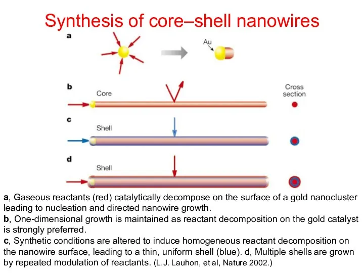
- 30. Synthesis of core–shell nanowires a, Gaseous reactants (red) catalytically decompose on the surface of a gold
- 31. Si–Si homoepitaxial core–shell nanowires. a, b, Diffraction contrast and highresolution TEM images, respectively, of an unannealed
- 32. Ge–Si core–shell nanowires
- 33. Si–Ge and Si–Ge–Si core–shell nanowires. Elemental mapping cross-section indicating a 21-nm-diameter Si core (blue circles), 10-nm
- 34. Coaxially-gated nanowire transistors a, Device schematic showing transistor structure. The inset shows the cross-section of the
- 36. Скачать презентацию
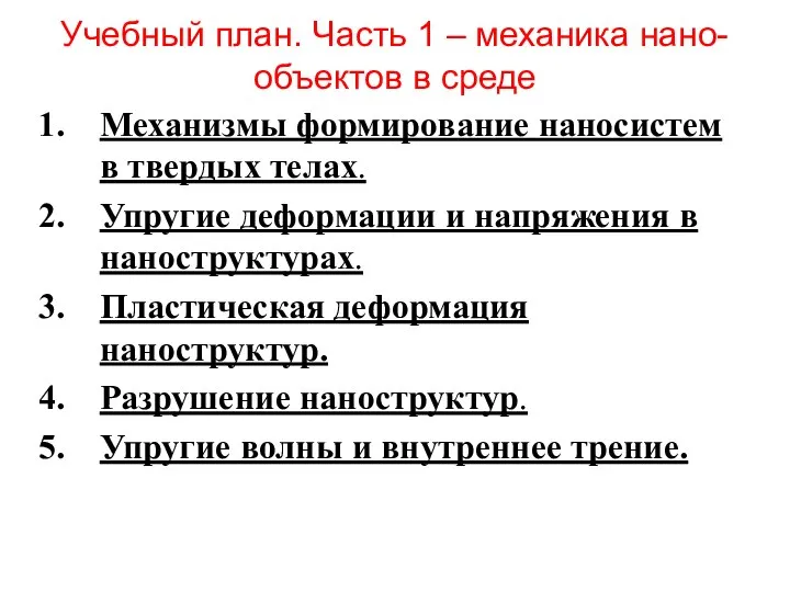
Учебный план. Часть 1 – механика нано-объектов в среде
Механизмы формирование наносистем
Учебный план. Часть 1 – механика нано-объектов в среде
Механизмы формирование наносистем

Учебный план. Часть 2 – нано-электро-механические системы
Материалы и технология изготовления нано-электро-механических
Учебный план. Часть 2 – нано-электро-механические системы
Материалы и технология изготовления нано-электро-механических

Литература
Основная
Cleland A.N. “Foundations of Nanomechanics” (Springer-Verlag, Berlin, Heidelberg, New York, 2003).
Freund
Литература
Основная
Cleland A.N. “Foundations of Nanomechanics” (Springer-Verlag, Berlin, Heidelberg, New York, 2003).
Freund
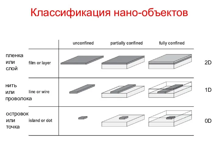
Классификация нано-объектов
пленка
или
слой
нить
или
проволока
островок
или
точка
1D
2D
0D
Классификация нано-объектов
пленка
или
слой
нить
или
проволока
островок
или
точка
1D
2D
0D
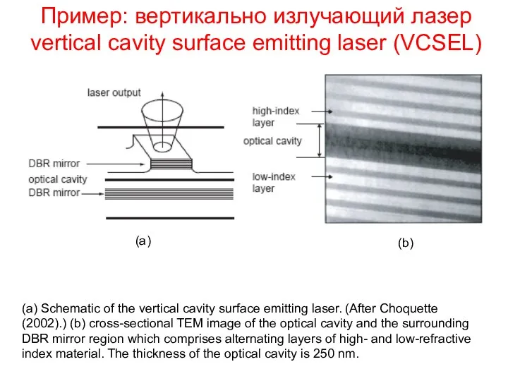
Пример: вертикально излучающий лазер
vertical cavity surface emitting laser (VCSEL)
(a) Schematic of
Пример: вертикально излучающий лазер
vertical cavity surface emitting laser (VCSEL)
(a) Schematic of
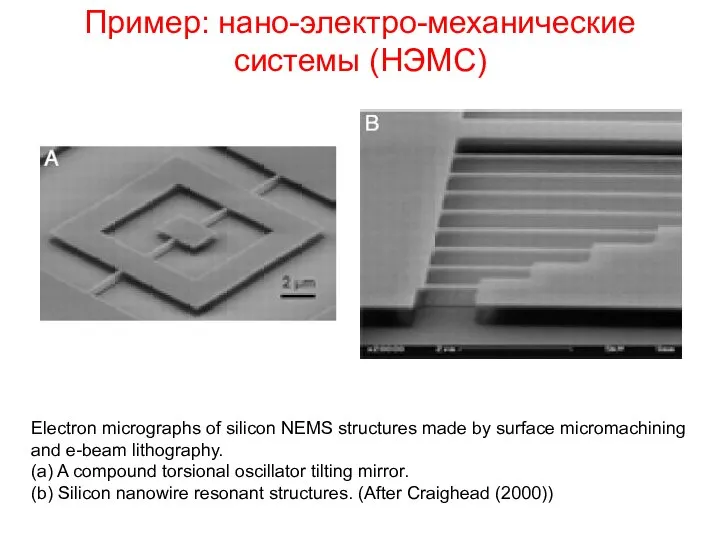
Пример: нано-электро-механические системы (НЭМС)
Electron micrographs of silicon NEMS structures made by
Пример: нано-электро-механические системы (НЭМС)
Electron micrographs of silicon NEMS structures made by
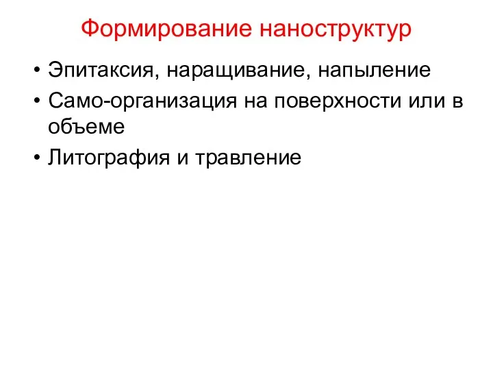
Формирование наноструктур
Эпитаксия, наращивание, напыление
Само-организация на поверхности или в объеме
Литография и травление
Формирование наноструктур
Эпитаксия, наращивание, напыление
Само-организация на поверхности или в объеме
Литография и травление

Планарные технологии
Планарные технологии
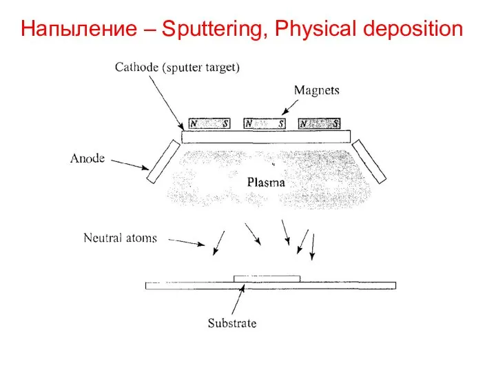
Напыление – Sputtering, Physical deposition
Напыление – Sputtering, Physical deposition
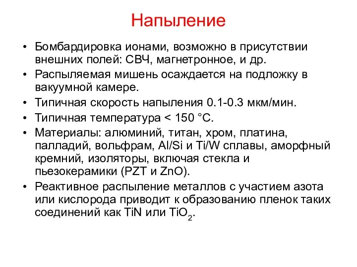
Напыление
Бомбардировка ионами, возможно в присутствии внешних полей: СВЧ, магнетронное, и др.
Распыляемая
Напыление
Бомбардировка ионами, возможно в присутствии внешних полей: СВЧ, магнетронное, и др.
Распыляемая
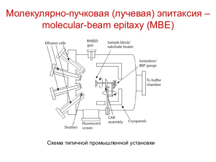
Молекулярно-пучковая (лучевая) эпитаксия – molecular-beam epitaxy (MBE)
Схема типичной промышленной установки
Молекулярно-пучковая (лучевая) эпитаксия – molecular-beam epitaxy (MBE)
Схема типичной промышленной установки

Процессы на поверхности при МПЭ
Процессы на поверхности при МПЭ
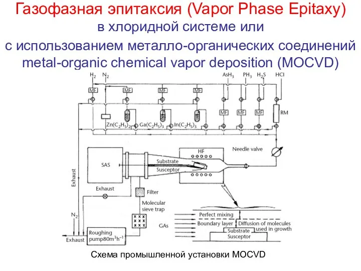
Газофазная эпитаксия (Vapor Phase Epitaxy)
в хлоридной системе или
с использованием металло-органических
Газофазная эпитаксия (Vapor Phase Epitaxy) в хлоридной системе или с использованием металло-органических
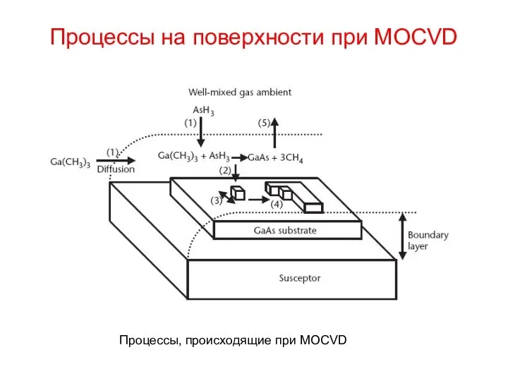
Процессы на поверхности при MOCVD
Процессы, происходящие при MOCVD
Процессы на поверхности при MOCVD
Процессы, происходящие при MOCVD
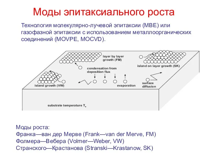
Моды эпитаксиального роста
Технология молекулярно-лучевой эпитаксии (MBE) или газофазной эпитаксии с использованием
Моды эпитаксиального роста
Технология молекулярно-лучевой эпитаксии (MBE) или газофазной эпитаксии с использованием

Движущая сила эпитаксии – пересыщение (supersaturation) газовой фазы и адсорбционного слоя
ΔF
Движущая сила эпитаксии – пересыщение (supersaturation) газовой фазы и адсорбционного слоя
ΔF
Само-организация
Само-организация
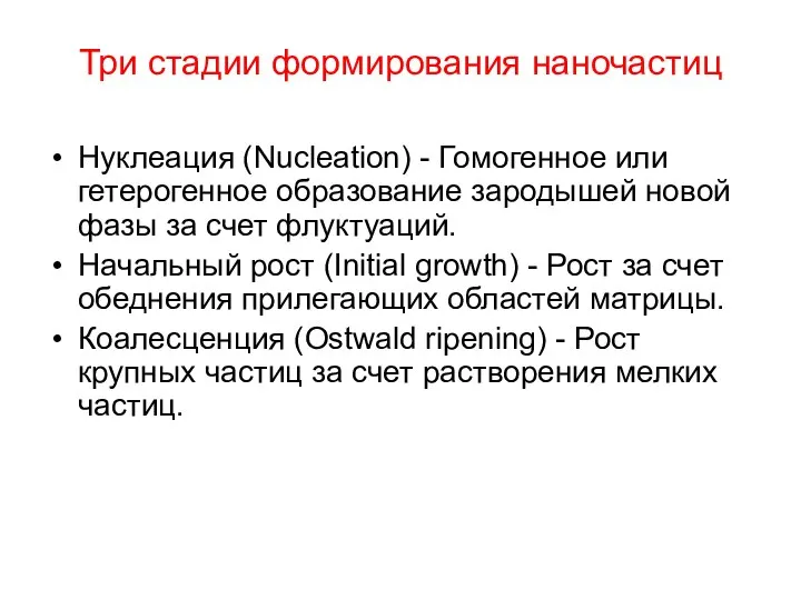
Три стадии формирования наночастиц
Нуклеация (Nucleation) - Гомогенное или гетерогенное образование зародышей
Три стадии формирования наночастиц
Нуклеация (Nucleation) - Гомогенное или гетерогенное образование зародышей
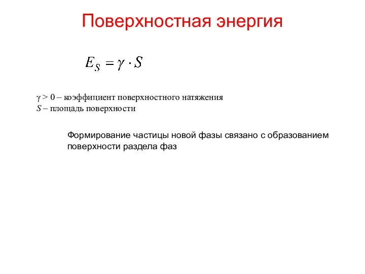
Поверхностная энергия
γ > 0 – коэффициент поверхностного натяжения
S – площадь поверхности
Формирование
Поверхностная энергия
γ > 0 – коэффициент поверхностного натяжения
S – площадь поверхности
Формирование

Нуклеация в объеме
Работа, необходимая для создания зародыша новой фазы
Критический зародыш
Вероятность
Нуклеация в объеме
Работа, необходимая для создания зародыша новой фазы
Критический зародыш
Вероятность

Нуклеация островка на поверхности
Young 1805
θ > 0 – распад пленки на
Нуклеация островка на поверхности
Young 1805
θ > 0 – распад пленки на
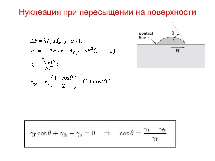
Нуклеация при пересыщении на поверхности
Нуклеация при пересыщении на поверхности
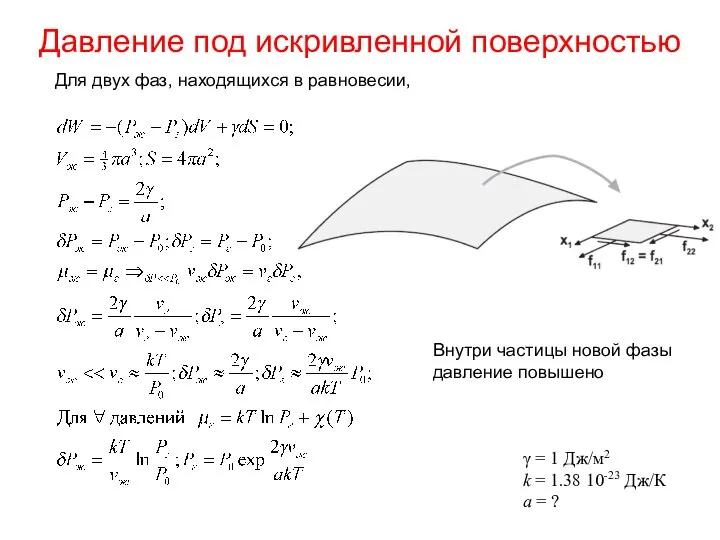
Давление под искривленной поверхностью
Для двух фаз, находящихся в равновесии,
γ = 1
Давление под искривленной поверхностью
Для двух фаз, находящихся в равновесии,
γ = 1
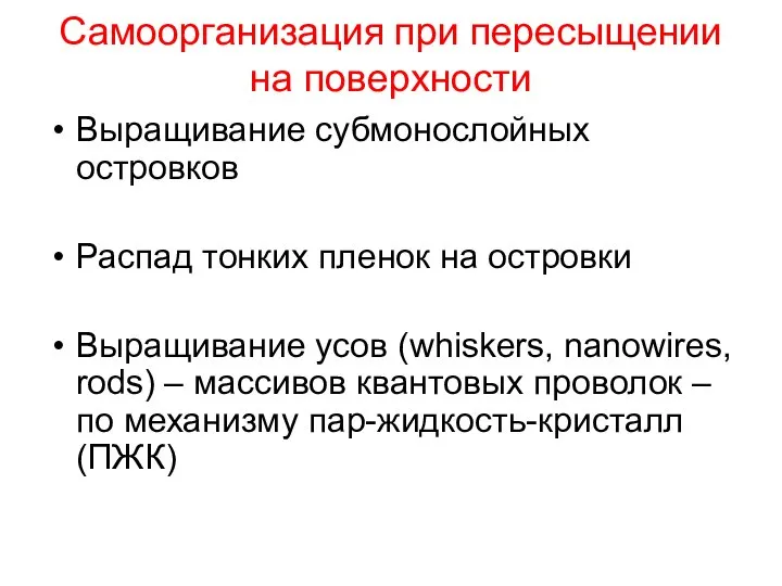
Самоорганизация при пересыщении на поверхности
Выращивание субмонослойных островков
Распад тонких пленок на
Самоорганизация при пересыщении на поверхности
Выращивание субмонослойных островков
Распад тонких пленок на

Механизм роста ПЖК
Пересыщенный пар
кристаллическая
подложка
пересыщенная жидкость
кристалл
ус
whisker
nanowire
nanorod
Механизм роста ПЖК
Пересыщенный пар
кристаллическая
подложка
пересыщенная жидкость
кристалл
ус
whisker
nanowire
nanorod
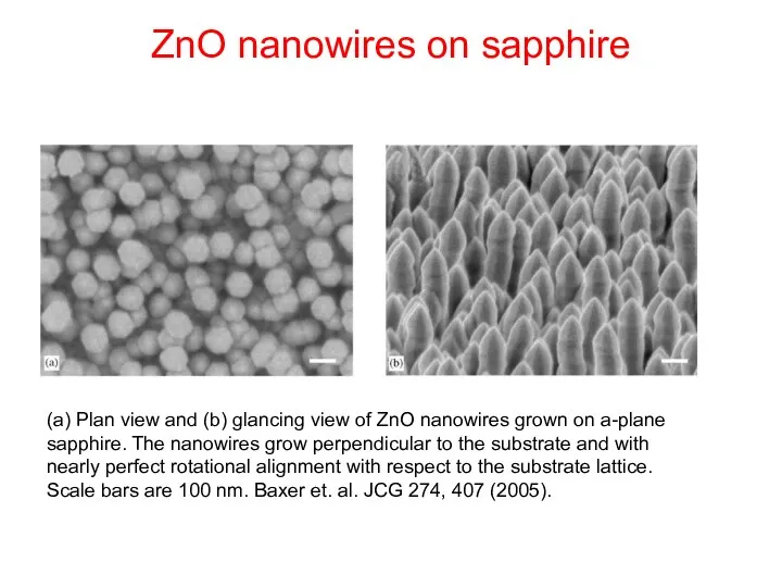
ZnO nanowires on sapphire
(a) Plan view and (b) glancing view of
ZnO nanowires on sapphire
(a) Plan view and (b) glancing view of
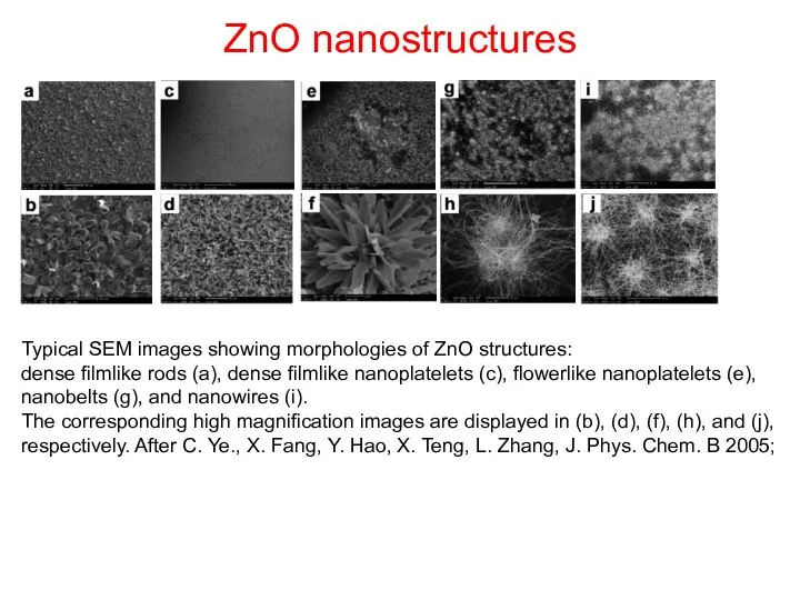
ZnO nanostructures
Typical SEM images showing morphologies of ZnO structures:
dense filmlike
ZnO nanostructures
Typical SEM images showing morphologies of ZnO structures:
dense filmlike
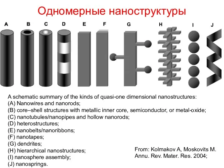
Одномерные наноструктуры
G
H
I
J
A schematic summary of the kinds of quasi-one dimensional nanostructures:
Одномерные наноструктуры
G
H
I
J
A schematic summary of the kinds of quasi-one dimensional nanostructures:
Synthesis of core–shell nanowires
a, Gaseous reactants (red) catalytically decompose on the
Synthesis of core–shell nanowires
a, Gaseous reactants (red) catalytically decompose on the
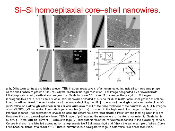
Si–Si homoepitaxial core–shell nanowires.
a, b, Diffraction contrast and highresolution TEM images,
Si–Si homoepitaxial core–shell nanowires.
a, b, Diffraction contrast and highresolution TEM images,

Ge–Si core–shell nanowires
Ge–Si core–shell nanowires
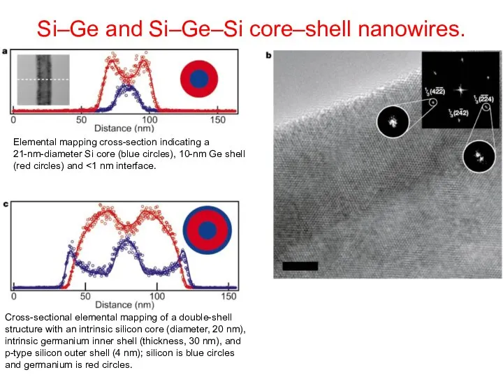
Si–Ge and Si–Ge–Si core–shell nanowires.
Elemental mapping cross-section indicating a 21-nm-diameter Si
Si–Ge and Si–Ge–Si core–shell nanowires.
Elemental mapping cross-section indicating a 21-nm-diameter Si
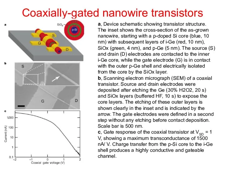
Coaxially-gated nanowire transistors
a, Device schematic showing transistor structure. The inset shows
Coaxially-gated nanowire transistors
a, Device schematic showing transistor structure. The inset shows
 Георгий Остер Задачник по физике
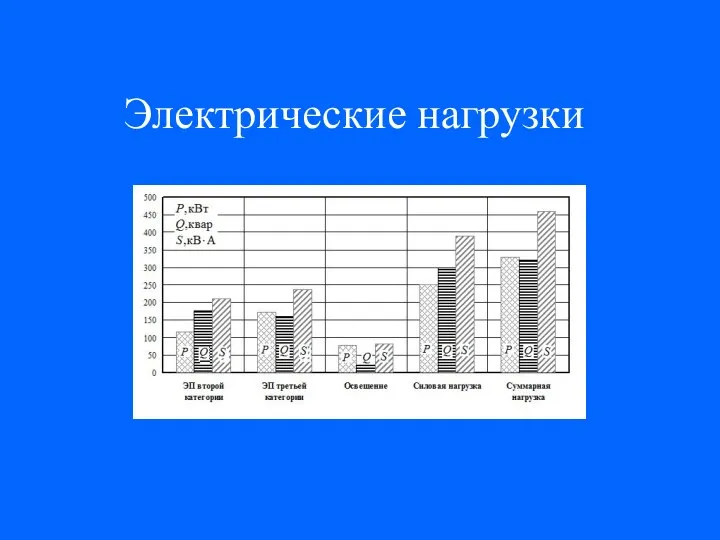 Электрические нагрузки. (Лекция 6)
 Электромагнитные излучения небесных тел
 Трение. (Тема 1.6)
 Система единиц СИ
 Рабочие жидкости гидросистем и их свойства. Выбор рабочих жидкостей и требования к ним. (Лекция 2)
 Законы Кирхгофа
 Машины и оборудование для сортировки и мойки каменных материалов. Лекция 7
 Счётчик Гейгера
  Свойства проводников и электроизоляционных материалов (тема 1.2)
 Эванджелиста Торричелли (1608-1647),
 Сила — векторная величина
 Откуда берется электрический ток?
 Метрология как наука. Её значение, цель, задачи, функции
 Небольшое небесное тело комета
 Термодинамические потоки. Явление переноса в газах: диффузия, теплопроводность и вязкость. Эффузия в разреженном газе
 Экспериментальные методы исследования частиц
 Презентация по физике "МагматизМ" - скачать бесплатно
 Қанның реологиялық қасиеттері. (Дәріс 12)
 Гамма-излучение
 Симметричный вибратор. Антенно-фидерные устройства и распространение радиоволн. Лекция № 4
 Аттестационная работа. Определение плотности морской ракушки и условий плавания ракушек в соленой и пресной воде
 Сопротивления в цепи переменного тока
 Увлекательная физика
 Элементы релятивистской механики
 Интегрированный урок: География с элементами физики
 Бесконтактные методы контроля температуры
 Эмиссионный микроспектральный анализ с лазерным отбором пробы