- Identification of Defects and Secondary Phases in Reactively Sputtered Cu2 ZnSnS4 Thin Films

Содержание
- 2. Outline Motivation Problems with characterization of thin films Experimental approach Results X-ray diffraction Raman Spectroscopy Transmission
- 3. Motivation – Phase Equilibrium CZTS is a line compound between Cu2SnS3 and ZnS Theoretically even a
- 4. Motivation – Crystal Structure Crystal structures of secondary phases similar to CZTS All primary peaks overlap
- 5. Experimental Approach Substrate Cu Zn Sn Introduce H2S into chamber during sputter deposition Sulfur is incorporated
- 6. Characterization - XRD Varying Zn/(Cu+Sn) Ratio Zn/(Cu+Sn) ratio is varied while holding Cu/Sn ratio constant Impossible
- 7. Characterization - XRD Varying Cu/(Zn+Sn) Ratio Cu/(Zn+Sn) ratio is varied while holding Zn/Sn ratio constant Need
- 8. Characterization – Raman Varying Zn/(Cu+Sn) Ratio Raman spectra show only minor changes even though composition is
- 9. Device Fabrication Glass Substrate 3000 µm Molybdenum Layer 1 µm 1.75 µm CdS (n-type) 55 nm
- 10. Device Characterization I-V Measurement EQE Measurement First CZTS devices grown by a reactive sputtering process Efficiency
- 11. Characterization - TEM 500nm Detrimental secondary phase interspersed in CZTS matrix Stacking faults in the secondary
- 12. Characterization - Auger Raster beam over sputtered surface of sample and scan for Cu, Zn, Sn
- 13. Characterization - CdZnS Cd penetration into ZnS lowers the cubic-hexagonal transition temperature Stacking faults in TEM
- 14. Characterization - Auger Sn Cd Overlay Sn and Cd signal Cd ion exchanges with Zn during
- 15. Summary CZTS thin films were grown using Reactive Sputtering Films were characterized using X-ray Diffraction and
- 16. Acknowledgements US Department of Energy, Office of Basic Energy Sciences as part of an Energy Frontier
- 18. Скачать презентацию

Outline
Motivation
Problems with characterization of thin films
Experimental approach
Results
X-ray diffraction
Raman Spectroscopy
Transmission Electron Microscopy
Scanning
Outline
Motivation
Problems with characterization of thin films
Experimental approach
Results
X-ray diffraction
Raman Spectroscopy
Transmission Electron Microscopy
Scanning

Motivation – Phase Equilibrium
CZTS is a line compound between Cu2SnS3 and
Motivation – Phase Equilibrium
CZTS is a line compound between Cu2SnS3 and

Motivation – Crystal Structure
Crystal structures of secondary phases similar to CZTS
All
Motivation – Crystal Structure
Crystal structures of secondary phases similar to CZTS
All

Experimental Approach
Substrate
Cu
Zn
Sn
Introduce H2S into chamber during sputter deposition
Sulfur is incorporated into
Experimental Approach
Substrate
Cu
Zn
Sn
Introduce H2S into chamber during sputter deposition
Sulfur is incorporated into

Characterization - XRD
Varying Zn/(Cu+Sn) Ratio
Zn/(Cu+Sn) ratio is varied while holding Cu/Sn
Characterization - XRD
Varying Zn/(Cu+Sn) Ratio
Zn/(Cu+Sn) ratio is varied while holding Cu/Sn

Characterization - XRD
Varying Cu/(Zn+Sn) Ratio
Cu/(Zn+Sn) ratio is varied while holding Zn/Sn
Characterization - XRD
Varying Cu/(Zn+Sn) Ratio
Cu/(Zn+Sn) ratio is varied while holding Zn/Sn

Characterization – Raman
Varying Zn/(Cu+Sn) Ratio
Raman spectra show only minor changes even
Characterization – Raman
Varying Zn/(Cu+Sn) Ratio
Raman spectra show only minor changes even

Device Fabrication
Glass Substrate
3000 µm
Molybdenum Layer
1 µm
1.75 µm
CdS (n-type)
55 nm
ZnO:Al (n-type)
340 nm
Aluminum
Device Fabrication
Glass Substrate
3000 µm
Molybdenum Layer
1 µm
1.75 µm
CdS (n-type)
55 nm
ZnO:Al (n-type)
340 nm
Aluminum

Device Characterization
I-V Measurement
EQE Measurement
First CZTS devices grown by a reactive sputtering
Device Characterization
I-V Measurement
EQE Measurement
First CZTS devices grown by a reactive sputtering

Characterization - TEM
500nm
Detrimental secondary phase interspersed in CZTS matrix
Stacking faults in
Characterization - TEM
500nm
Detrimental secondary phase interspersed in CZTS matrix
Stacking faults in

Characterization - Auger
Raster beam over sputtered surface of sample and scan
Characterization - Auger
Raster beam over sputtered surface of sample and scan

Characterization - CdZnS
Cd penetration into ZnS lowers the cubic-hexagonal transition temperature
Stacking
Characterization - CdZnS
Cd penetration into ZnS lowers the cubic-hexagonal transition temperature
Stacking

Characterization - Auger
Sn
Cd
Overlay Sn and Cd signal
Cd ion exchanges with Zn
Characterization - Auger
Sn
Cd
Overlay Sn and Cd signal
Cd ion exchanges with Zn

Summary
CZTS thin films were grown using Reactive Sputtering
Films were characterized using
Summary
CZTS thin films were grown using Reactive Sputtering
Films were characterized using

Acknowledgements
US Department of Energy, Office of Basic Energy Sciences as part
Acknowledgements
US Department of Energy, Office of Basic Energy Sciences as part
 Годівля овець
 National anthem of Іndia
 Богословское обоснование трезвенного движения
 фразовый глагол make Save the Earth
 Пространственные концепции
 Салон красоты Экспресс-макияж
 Исследование образцов стали ВКС-10
 Презентация по правосознанию
 Проект: Профессии
 Машиноведение. История создания швейных машин. Виды приводов
 Регламент формирования сводных годовых и месячных графиков ремонтов устройств РЗА-объектов
 Технология обойных работ
 Педагогика. Психология
 8_задание_Никольская
 20120122_smuta_7_klass
 Электроизмерительные приборы. Часть 1.1
 Технология изготовления валов
 презентация по деятельности психологтческой службы 2022-2023
 Лепка из глины Вазы - 3 вида
 Самоменеджмент_л
 Агентство поздравлений
 malenkie_tragedii
 Центр гигиены и эпидемиологии по железнодорожному транспорту
 Корзины
 С Днём Энергетика!!!
 По страницам любимых сказок
 Здоровье
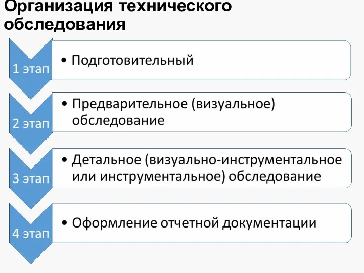 Организация технического обследования