- Field programmable gate arrays

Содержание
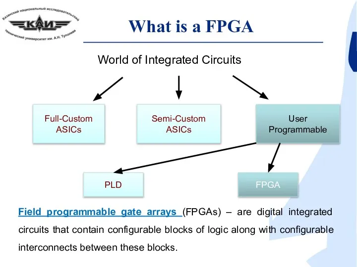
- 2. What is a FPGA Field programmable gate arrays (FPGAs) – are digital integrated circuits that contain
- 3. Why do we need FPGAs? Low development cost Short time to market Reprogrammable High performance ASICs
- 4. Other FPGA advantages Manufacturing cycle for ASIC is very costly, lengthy and engages lots of manpower
- 5. Architecture of FPGA The architecture of FPGA is very simple than other programmable devices Elements of
- 6. A simple modern architecture of FPGA is shown below: Architecture of FPGA All FPGAs include a
- 7. A simple programmable function
- 8. Technology of program logic devices Fusible link technologies Unprogrammed fusible links Programmed fusible links
- 9. Technology of program logic devices Antifuse technologies Unprogrammed antifuse links Programmed antifuse links The act of
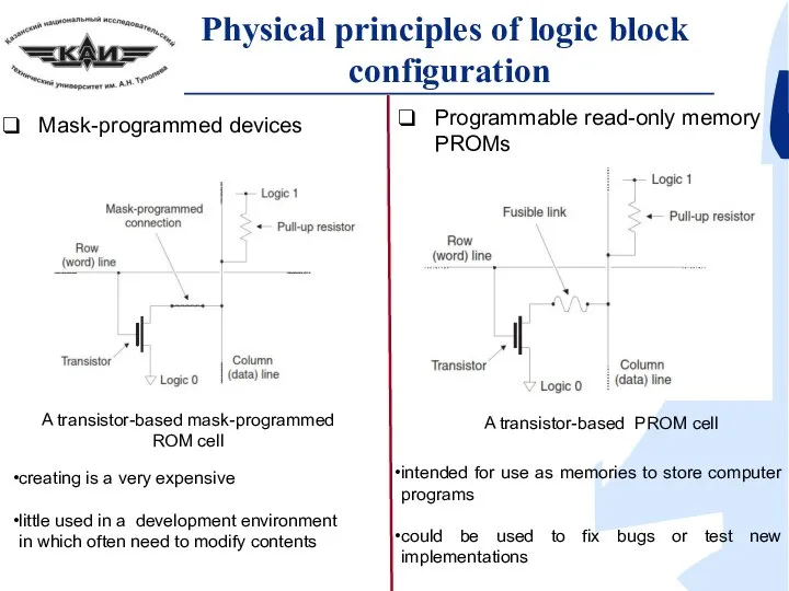
- 10. Physical principles of logic block configuration Mask-programmed devices A transistor-based mask-programmed ROM cell creating is a
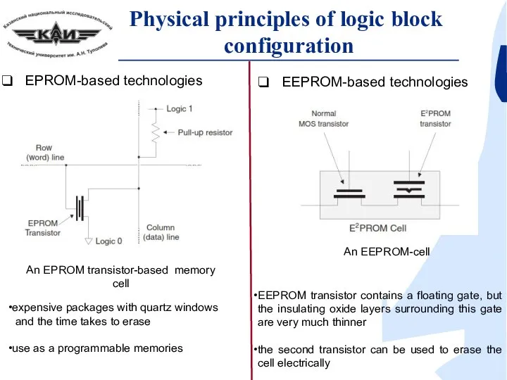
- 11. Physical principles of logic block configuration EPROM-based technologies An EPROM transistor-based memory cell expensive packages with
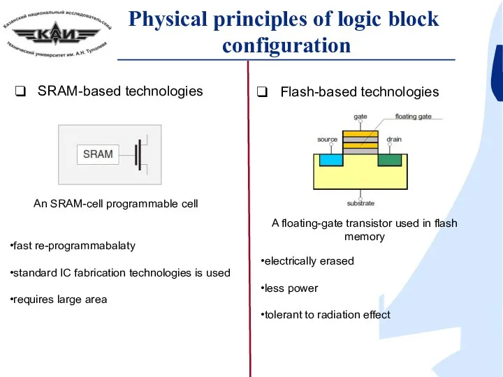
- 12. Physical principles of logic block configuration fast re-programmabalaty standard IC fabrication technologies is used requires large
- 14. Скачать презентацию
What is a FPGA
Field programmable gate arrays (FPGAs) – are
What is a FPGA
Field programmable gate arrays (FPGAs) – are
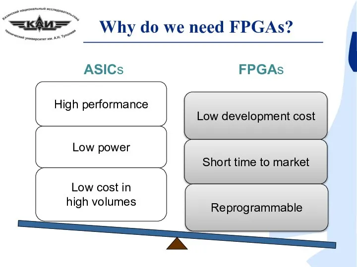
Why do we need FPGAs?
Low development cost
Short time to market
Reprogrammable
High performance
ASICs
FPGAs
Low
Why do we need FPGAs?
Low development cost
Short time to market
Reprogrammable
High performance
ASICs
FPGAs
Low
Other FPGA advantages
Manufacturing cycle for ASIC is very costly, lengthy and
Other FPGA advantages
Manufacturing cycle for ASIC is very costly, lengthy and
Architecture of FPGA
The architecture of FPGA is very simple than other
Architecture of FPGA
The architecture of FPGA is very simple than other
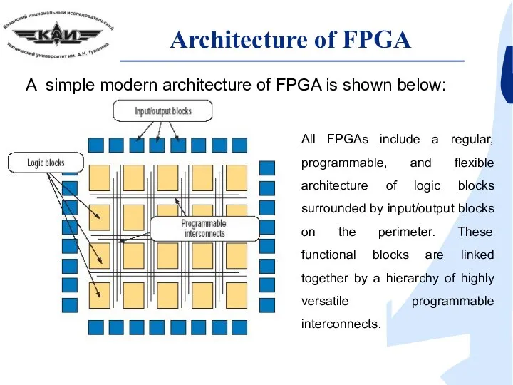
A simple modern architecture of FPGA is shown below:
Architecture of FPGA
All
A simple modern architecture of FPGA is shown below:
Architecture of FPGA
All
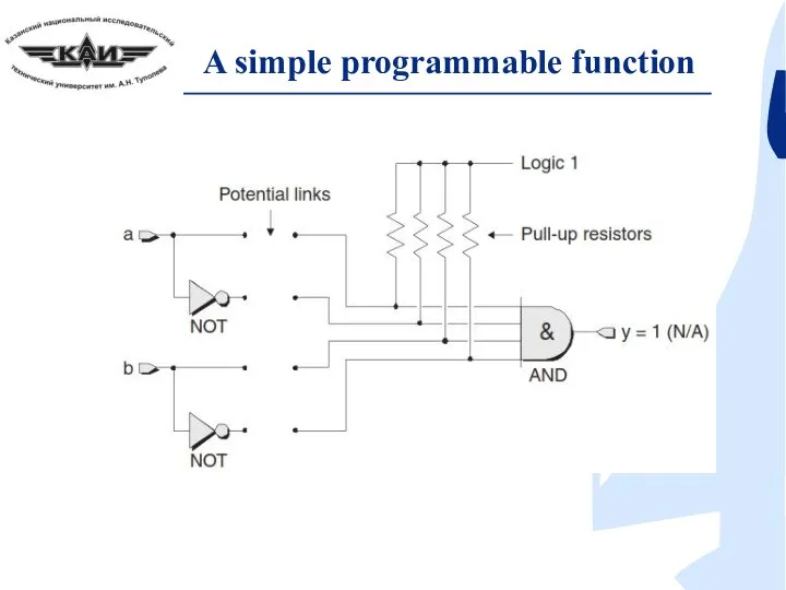
A simple programmable function
A simple programmable function
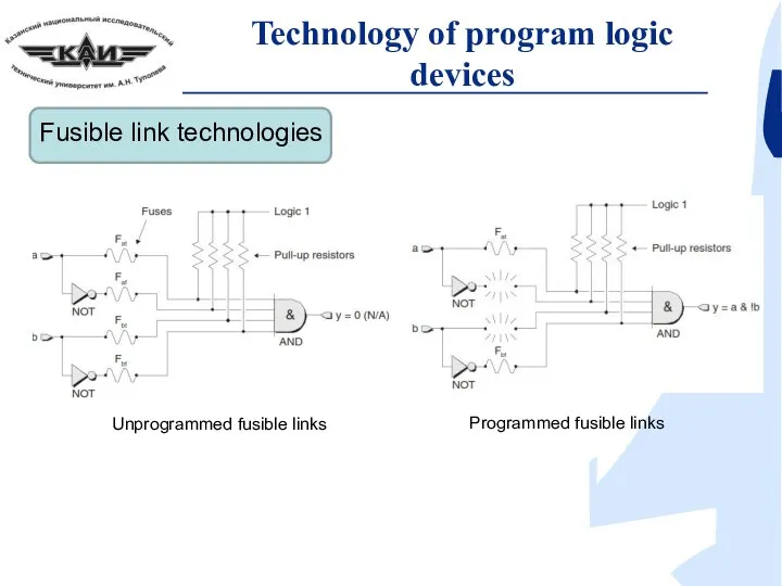
Technology of program logic devices
Fusible link technologies
Unprogrammed fusible links
Programmed fusible links
Technology of program logic devices
Fusible link technologies
Unprogrammed fusible links
Programmed fusible links
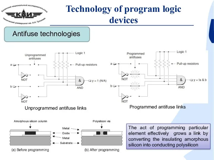
Technology of program logic devices
Antifuse technologies
Unprogrammed antifuse links
Programmed antifuse links
The act
Technology of program logic devices
Antifuse technologies
Unprogrammed antifuse links
Programmed antifuse links
The act
Physical principles of logic block
configuration
Mask-programmed devices
A transistor-based mask-programmed
ROM cell
Physical principles of logic block
configuration
Mask-programmed devices
A transistor-based mask-programmed
ROM cell
Physical principles of logic block
configuration
EPROM-based technologies
An EPROM transistor-based memory cell
Physical principles of logic block
configuration
EPROM-based technologies
An EPROM transistor-based memory cell
Physical principles of logic block
configuration
fast re-programmabalaty
standard IC fabrication technologies
Physical principles of logic block
configuration
fast re-programmabalaty
standard IC fabrication technologies
 Состояние и перспективы развития горнолыжного туризма в России
 Презентация "Экономический рост России и ее интеллектуальный потенциал" - скачать презентации по Экономике
 кач. реакции на белки
 ЭЛЬ ГРЕКО (1541-1614)
  Единая автоматизированная информационная система (ЕАИС) ФТС России
  Особенности спортивного коллектива
 Лекция 7 Уравнение множественной регрессии Теорема Гаусса-Маркова Автор: Костюнин Владимир Ильич, доцент кафедры: «Математ
 My idol Lionel Andrés Messi
 Проектная работа по немецкому языку. Немецкие автомобили
 Великие математики
 День флага и герба Крыма
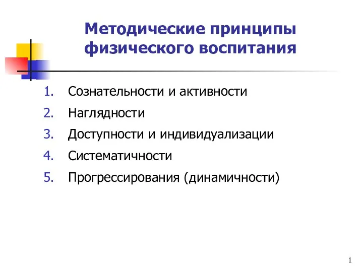 Методические принципы физического воспитания
  Лекция 3 Электропроводность растворов электролитов
 Презентация Изучение проблемных областей государственного регулирования.
 Коммуникационные сети
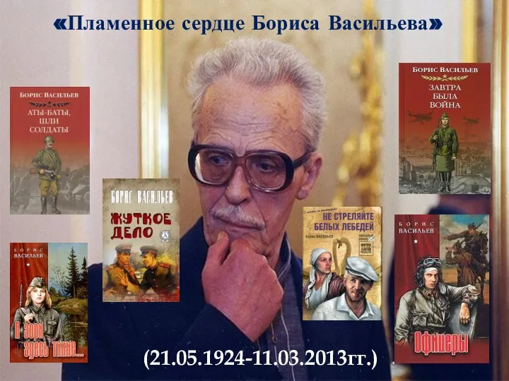 Пламенное сердце Бориса Васильева
 Электрические измерения и приборы
 Презентация Анализ валютного рынка России
  Тема: «Вклад Фридриха Августа фон Хайека в современную экономическую науку»
  Университетский класс: цели и задачи, организация деятельности В.Ю.Болтнев, директор школы
 Аудиовизуальные и технические средства обучения. Телевизор
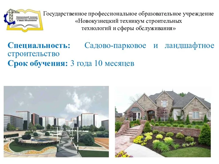 Садово-парковое и ландшафтное строительство
 синий - презентация для начальной школы
 Объекты JavaScript
 Киберспорт – это спорт
 Единицы длины и их соотношение - презентация для начальной школы
 Культура движения
 Проект коттеджного дома