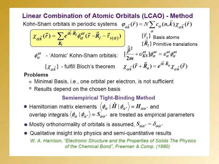
- Practical application of the method of Kona-Shema. Pseudopotentials method

Содержание
- 7. Выводы
- 24. The large number of surface structures observed on III-V (001) surfaces have early on prompted attempts
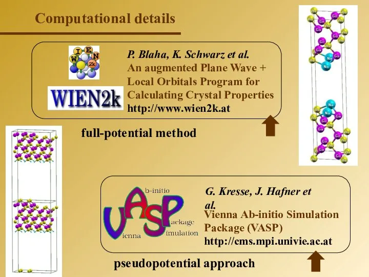
- 25. Computational details P. Blaha, K. Schwarz et al. An augmented Plane Wave + Local Orbitals Program
- 26. * - S.Lee, S. Lee, M. Scheffler. PRB 69, 125317 (2004) (FHI) ** - G. Qian,
- 27. Models of Ga-terminated GaAs(001)-(4х2) surface
- 28. ELECTRONIC STRUCTURE Two dimensional Brillouin zone (a) and E(k) for Ga-terminated β2- (b) and ζ-GaAs(001)-(4×2) (c),
- 29. ζ-GaAs(001)-(4×2) Adsorption on ζ-GaAs(001)-(4×2) The position of adsorbates (cesium and chlorine) on surface ζ-GaAs(001)-(4×2) after relaxation
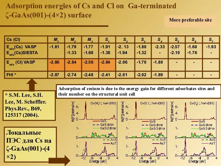
- 30. Adsorption energies of Cs and Cl on Ga-terminated ζ-GaAs(001)-(4×2) surface * S.M. Lee, S.H. Lee, M.
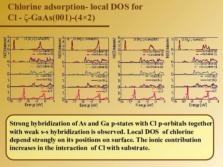
- 31. Strong hybridization of As and Ga p-states with Cl p-orbitals together with weak s-s hybridization is
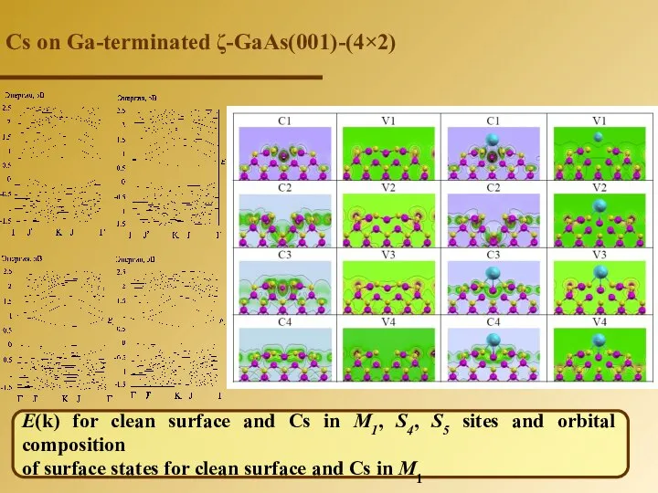
- 32. Cs on Ga-terminated ζ-GaAs(001)-(4×2) E(k) for clean surface and Cs in М1, S4, S5 sites and
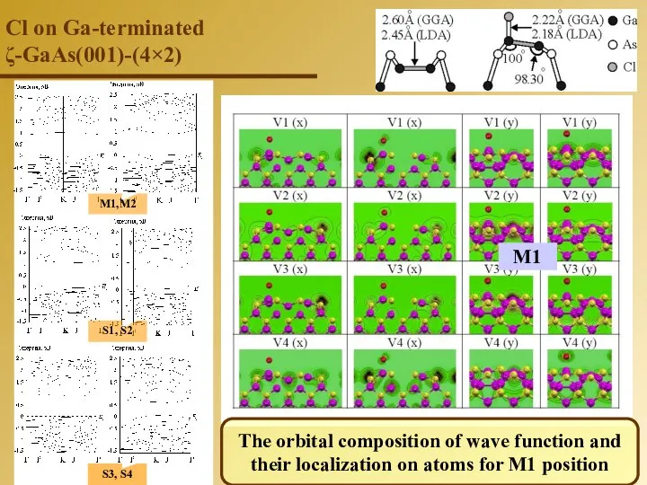
- 33. М1,М2 S1, S2 S3, S4 M1 The orbital composition of wave function and their localization on
- 34. The charge difference for Cs in M1 –M3, S1, S5, S6 positions on Ga- terminated ζ-GaAs(001)-(4×2).
- 35. The charge difference for Cl in M1 –M3, S1, S5, S6 positions on Ga-terminated ζ-GaAs(001)-(4×2). X
- 36. Charge transfer Integrated Cs valence charge difference as function of integration radius for different adsorption sites
- 37. The adsorption energies of Cs for S1 and S2 sites on ζ-GaAs(001)-(4×2) with adsorbed Cs in
- 38. Charge transfer Integrated valence charge difference as a function of spheres radius for ζ-GaAs(001)-(4×2) with two
- 39. Cs on ζ-GaAs(001)-(4×2) E(k) for ζ–GaAs(001)–(4×2) with Cs adsorbed in S5 site (a), with two Cs
- 40. Electronic structure of (Cs-O)/GaAs(001) interface Models of (Cs-O)/GaAs(001) interface Total, local surface DOS of ζ-GaAs(001)-(4×2) with
- 41. Calculated STM images of filled and empty states: I adsorbed in the M1 position on ζ-GaAs(001)-(4×2)
- 42. Calculated STM images: clean ζ-GaAs(001)-(4×2) U =-1.5 V (filled) U =1.8 V (empty) S.H. Lee et
- 44. Скачать презентацию


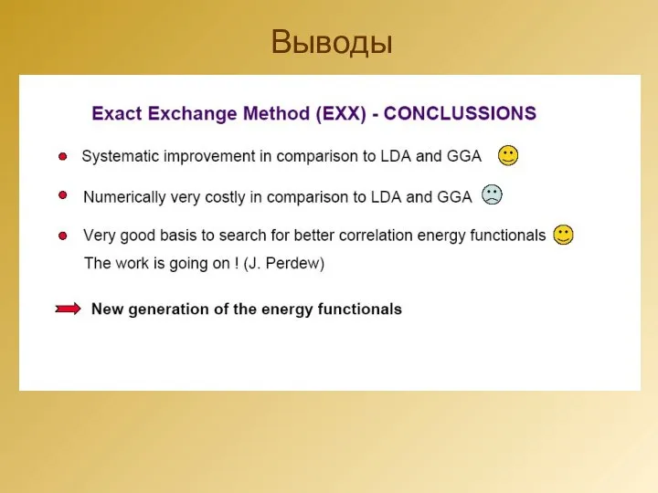
Выводы
Выводы


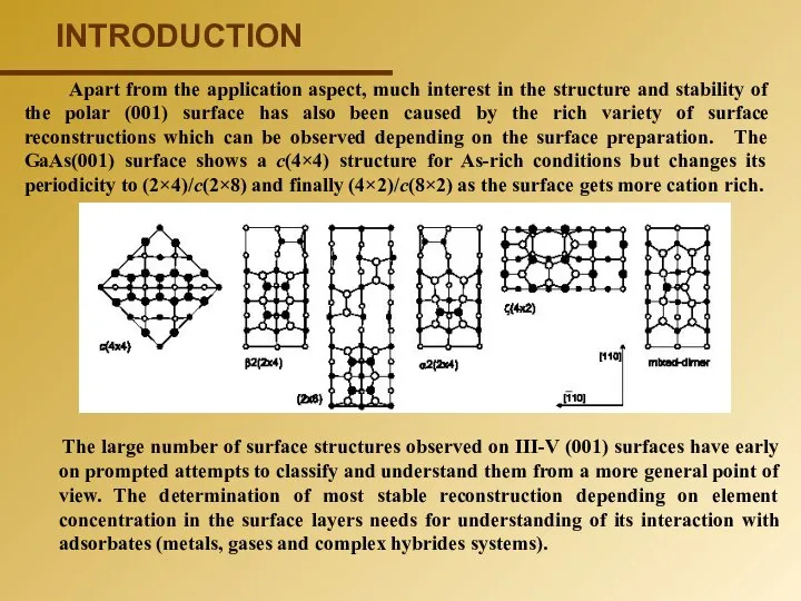
The large number of surface structures observed on III-V (001) surfaces
The large number of surface structures observed on III-V (001) surfaces
Computational details
P. Blaha, K. Schwarz et al.
An augmented Plane Wave
Computational details
P. Blaha, K. Schwarz et al.
An augmented Plane Wave
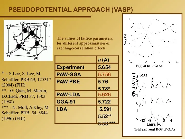
* - S.Lee, S. Lee, M. Scheffler. PRB 69, 125317 (2004)
* - S.Lee, S. Lee, M. Scheffler. PRB 69, 125317 (2004)
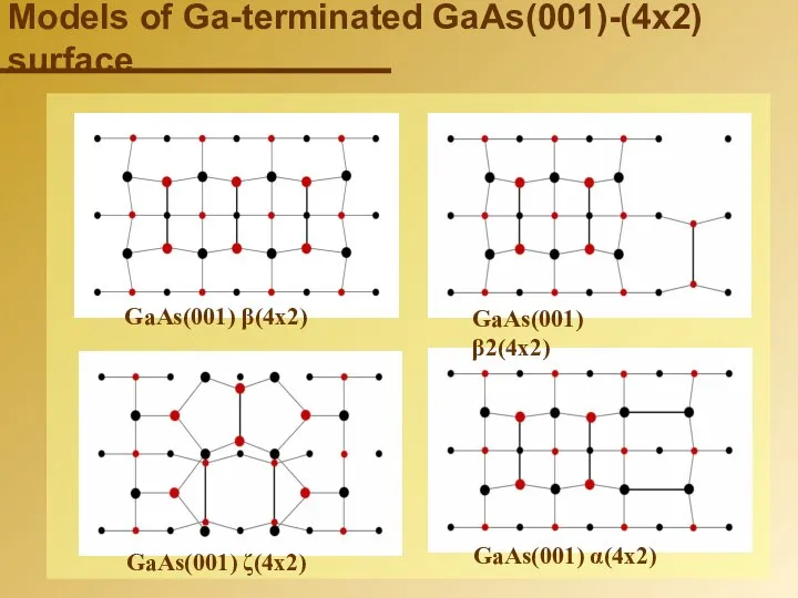
Models of Ga-terminated GaAs(001)-(4х2) surface
Models of Ga-terminated GaAs(001)-(4х2) surface
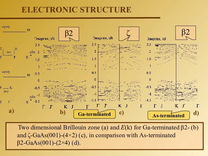
ELECTRONIC STRUCTURE
Two dimensional Brillouin zone (a) and E(k) for
ELECTRONIC STRUCTURE
Two dimensional Brillouin zone (a) and E(k) for

ζ-GaAs(001)-(4×2)
Adsorption on ζ-GaAs(001)-(4×2)
The position of adsorbates (cesium
ζ-GaAs(001)-(4×2)
Adsorption on ζ-GaAs(001)-(4×2)
The position of adsorbates (cesium
Adsorption energies
Adsorption energies
Strong hybridization of As and Ga p-states with Cl
Strong hybridization of As and Ga p-states with Cl
Cs on Ga-terminated ζ-GaAs(001)-(4×2)
E(k) for clean surface
Cs on Ga-terminated ζ-GaAs(001)-(4×2)
E(k) for clean surface
М1,М2
S1, S2
S3, S4
M1
The orbital composition of wave
М1,М2
S1, S2
S3, S4
M1
The orbital composition of wave

The charge difference for Cs in M1 –M3, S1, S5, S6
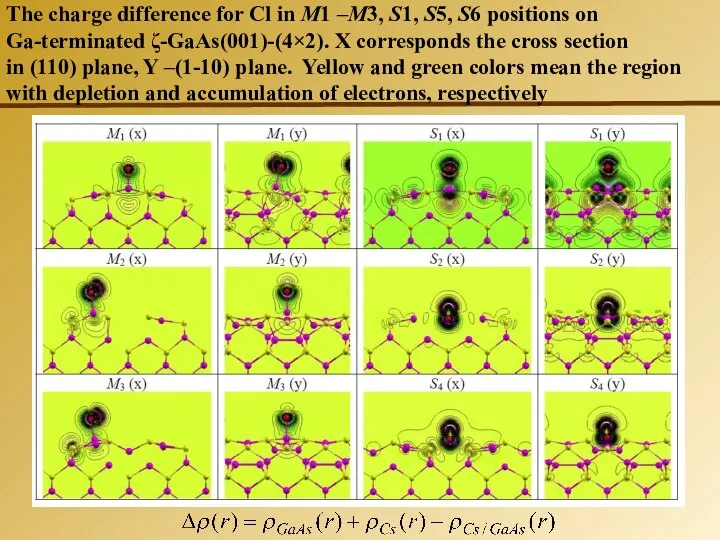
The charge difference for Cl in M1 –M3, S1, S5, S6
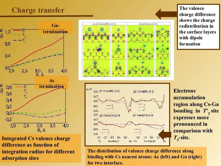
Charge transfer
Integrated Cs valence charge difference as function of integration radius
Charge transfer
Integrated Cs valence charge difference as function of integration radius
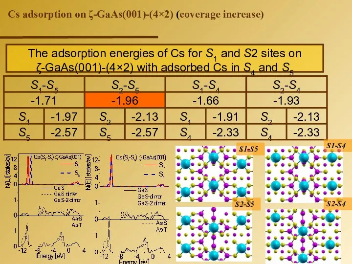
The adsorption energies of Cs for S1 and S2 sites on
The adsorption energies of Cs for S1 and S2 sites on
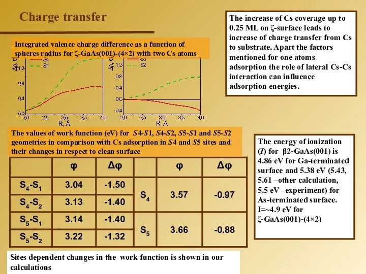
Charge transfer
Integrated valence charge difference as a function of spheres radius
Charge transfer
Integrated valence charge difference as a function of spheres radius
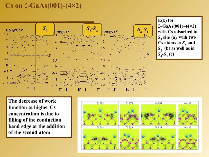
Cs on ζ-GaAs(001)-(4×2)
E(k) for ζ–GaAs(001)–(4×2) with Cs adsorbed in
Cs on ζ-GaAs(001)-(4×2)
E(k) for ζ–GaAs(001)–(4×2) with Cs adsorbed in
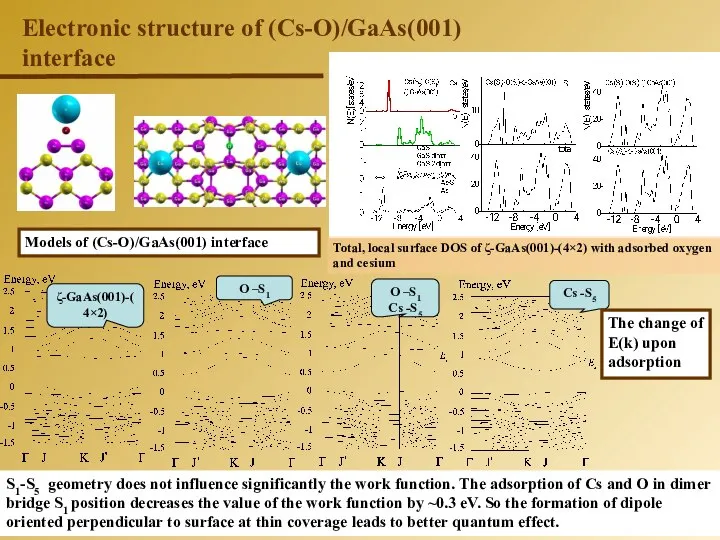
Electronic structure of (Cs-O)/GaAs(001) interface
Models of (Cs-O)/GaAs(001) interface
Electronic structure of (Cs-O)/GaAs(001) interface
Models of (Cs-O)/GaAs(001) interface
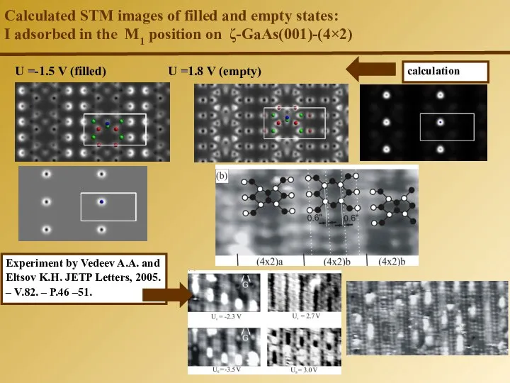
Calculated STM images of filled and empty states:
I adsorbed in the
Calculated STM images of filled and empty states:
I adsorbed in the
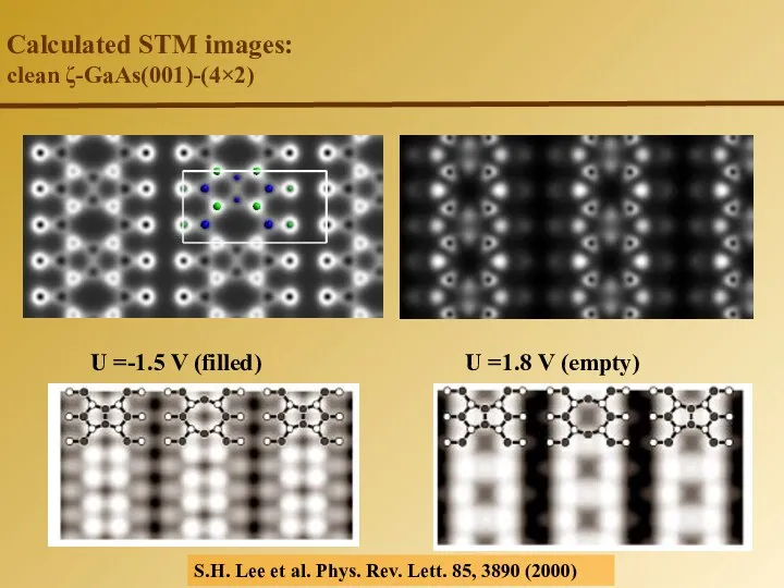
Calculated STM images:
clean ζ-GaAs(001)-(4×2)
U =-1.5 V (filled) U =1.8
Calculated STM images:
clean ζ-GaAs(001)-(4×2)
U =-1.5 V (filled) U =1.8
 Определители и их применения
 Текстовые задачи и пути их решения. Элективный курс. 9 класс
 Математика в профессии сварщика
 Комплексные числа
 Построение треугольников по заданным элемента
 Расчет площадей помещений. (Лекция 9.7)
 Векторная алгебра
 Презентация по математике "Урок математики. 2 класс." - скачать бесплатно
 Устный счет
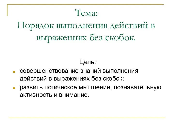 Тема: Порядок выполнения действий в выражениях без скобок. Цель: совершенствование знаний выполнения действий в выражениях без
  Вычитание чисел 5,6,7,8,9. Уменьшаемое, вычитаемое, разность
 Аппроксимация функций (тема 8)
 Мода и медиана
 Справочник по геометрии
 Презентация по математике "Графическое решение квадратных уравнений" - скачать
  Связь между координатами вектора и координатами его начала и конца
 Примеры на действия с алгебраическими дробями
 Целое уравнение и его корни. 9 класс
 Это мы не проходили… интеллектуально-познавательная игра
 Аттестационная работа. Рациональные способы устных вычислений
 Простейшие вероятностные задачи. Элементарные и сложные события. Вероятность противоположного события. (11 класс)
 Презентация по математике "тренажер" - скачать бесплатно
 Геометрия. Основные утверждения и теоремы
 Математика. Закрепление
 Организация познавательной деятельности учащихся в условиях интеграции математики с физикой
 Презентация по математике "ЧИСЛО И ЦИФРА 5" - скачать бесплатно
 Прибавление и вычитание числа 2 (Анимированная сорбонка)
 Презентация по математике "Окружность и круг" - скачать бесплатно