- Company confidential Lenovo S660 Service Manual

Содержание
- 2. Function Block
- 3. M/B Top Placement #1 MT6582 MCP Charge IC Audio Jack Receiver SKY77593 MT6166 FLASH LED IC
- 4. M/B Bottom Placement #2 MT6323 DUAL SIM CONNECTOR BACK UP BATTERY Mic 2 TF CARD CONNECTOR
- 5. BB Common Question BB-1 Power on failure (無法開機) BB-2 Firmware update failure (無法更新軟件) BB-3 Charging failure
- 6. BB-1 Can not power on (無法開機) (1/3) 1. Check if battery power level is low (確認電池是否有電?)
- 7. 5. Please check whether MT6323 voltage is normal (請確認MT6323周圍電壓是否正常?) VPROC_PMU should be between C134 (0.9V~1.1V) VSYS_PMU
- 8. BB-1 Can not power on (無法開機) (3/3) VCORE≈0.7V~1.3V VPORC≈0.7V~1.3V VIO18=1.8V VIO28=2.8V VM12_INT=1.2V VA1=2.5V VA2=2.5V VUSB=3.3V VTCXO=2.8V
- 9. BB-2 Can not download (無法更新軟件) (1/3) 1. Please check whether current is normal after boot (確認開機後電流起跳正常)
- 10. BB-2 Can not download (無法更新軟件) (2/3) 4. If DL is passed, and META mode is un-entered,
- 11. BB-2 Can not download (無法更新軟件) (3/3) 5. Check if com port is correct (確認com port是否正確)
- 12. BB-3 Can not charging (無法充電) (1/2) 1. Check if battery resistance R332 Pin1(BAT_ID) is 10kΩ when
- 13. BB-3 Can not charging (無法充電) (2/2) 4. Check charging IC and related circuit soldering condition is
- 14. BB-4 SIM Card Identification error (SIM卡無法識別) (1/2) 1. Check if SIM Card is in normal condition
- 15. BB-4 SIM Card Identification error (SIM卡無法識別) (2/2) SIM1和SIM2的DATA/RST/CLOCK单独分开使用 DATA/RST/CLOCK of SIM1 and SIM2 are used seperately
- 16. BB-5 Can not display (畫面無法顯示或顯示異常) 1. Check J904 soldering condition (確認J904是否有異狀[鍚短 or 空焊]?) 2. Replace LCD
- 17. G-sensor供电电压。该电压等同于VIO18,该电压异常系统就无法开起来,所以sensor不良不用check此电位。 G-Sensor voltage is as same as VIO18. if this voltage is in error, system will
- 18. BB-6 sensor function fail (感測器不良) (2/2) G-sensor I2C通過上拉電阻連接到CPU,此I2C與touch panel共用,VDD18_PMU異常會造成所有sensor fail。 G-sensor I2C connect to CPU with
- 19. BB-7 Touch Panel no function (無法觸屏) (1/2) 1. Check if TP connector is loosen (確認TP Connector
- 20. BB-7 Touch Panel no function (無法觸屏) (2/2) TP circuit TP工作電壓2.8V/1.8V TP Working Voltage 2.8v/1.8v 復位信號 Reset
- 21. BB-8 Vibrator no function (馬達無振動) 1. Check if motor is in normal condition (Resistance is 30Ω)
- 22. BB-9 Camera can not turn on (無法攝像) (1/4) 1. Check camera module has been well assembled
- 23. BB-9 Camera can not turn on (無法攝像) (2/4) 主camera的4組工作電壓均是由PMU LDO輸出通過給camera All 4 working voltage of main
- 24. BB-9 Camera can not turn on (無法攝像) (3/4) 1:無法進入拍攝模式,此為camera無法通過I2C信號被CPU正常識別造成,此不良主要查供電/reset/CLK/PWD是否正常 1. Camera shooting model is not accessible.
- 25. BB-9 Camera can not turn on (無法攝像) (4/4) VREF/HREF: Sensor垂直/水平參考信號 Sensor reference of horizon and vertical
- 26. BB-10 MIC no function (麥克風無作用) 1. 確認J1003 Microphone是否正常 (正常Mic阻抗約0.95KΩ) Check if J1003 Microphone is in normal
- 27. BB-11 Speaker no function (喇叭無聲) 1. 確認MB to SB FPC是否連接ok Check MB to SB FPC is
- 28. BB-12 Audio function fail (Audio 不良) (1/4) Audio类不良针对不同测试项fail,检查不同的路径. 1:wave play back fail?测的是SPK路径. 2:receiver fail ?测的是手机听筒路径. 3:headset
- 29. BB-12 Audio function fail (Audio 不良) (1/4) Speaker path: PMU給出SPK信號進入Audio PA 進行放大處理 PMU output SPK signal
- 30. BB-12 Audio function fail (Audio 不良) (2/4) Receiver path: Phone MIC path PMU輸出音頻信號 PMU output audio
- 31. BB-12 Audio function fail (Audio 不良) (3/4) 耳機左右聲道電路: Earphone L/R channel circuit PMU輸出耳機音頻信號 PMU output earphone
- 32. BB-12 Audio function fail (Audio 不良) (4/4) 耳機MIC電路 Earphone MIC Circuit: 為耳機MIC提供偏置電壓 Provide bias votage for
- 33. BB-13 SD Card no function (SD Card無作用) SD card 偵測信號 SD card signal detect SD card
- 34. WIFI/BT/GPS I/Q Signal SCLK,DataSignal Connect to CPU MT6582 獨立的26M TCXO,Output Clock to MT6627 Separate 26M TCXO,
- 35. MT6627 Power Supply WIFI/BT/GPS From PMU MT6323 Output to MT6627
- 36. GSM PA + Switch GSM Vbat GSM LB Tx input GSM HB Tx input WCDMA Band
- 37. GSM RX GSM HB/LB Circuit: 2G LB Rx 2G HB Rx Balance output to transceiver LB
- 38. WCDMA Band1/8 TRx (VV36/38) Tx from Transceiver Band 8 Tx Rx balance to transceiver TRx connect
- 39. WCDMA Band2/5 TRx (VV37) Tx from Transceiver Band 5 Tx Rx balance to transceiver TRx connect
- 40. RF introduction: MT6166 Function Block
- 41. RF introduction: MT6166 Pin assignment
- 42. RF introduction: Antenna Circuit Antenna Circuit RF天線主要包含了2G/3G/WIFI/GPS, 其匹配電路分別描述如下 RF antenna consists 2G/3G/WIFI/GPS, Description as right diagram
- 43. RF introduction:2G/3G Main Antenna Position
- 44. RF introduction: WIFI Antenna Position
- 45. RF common issue RF-1:Network function error RF-2:GSM problem RF-3:WCDMA problem RF-4:GSM/WCDMA Rx error RF-5:WIFI problem
- 46. RF-1:Network function error 若2G/3G 網路功能異常,請檢查螢幕天線格數,SIM card是否裝好? Coaxial cable和是否組好? If 2G/3G network is on failure, check reception
- 47. RF-2:GSM Trouble shooting (1/3) Check GSM transmission path (檢查GSM發射路徑) Tx I/Q Signal
- 48. RF-2:GSM Trouble shooting (2/3) GSM發射路徑 GSM transmission path 由於2G PA和ASM整合在U1302,檢查發射時對應邏輯控制電壓是否正確 Due to 2G PA and ASM
- 49. RF-2:GSM Trouble shooting (3/3) GSM發射路徑 GSM transmission path 檢查發射路徑的功率 check power of transmission path 使用spectrum probe量測下列標駐點,測量其功率
- 50. RF-3:WCDMA Trouble shooting (1/5) WCDMA發射路徑 WCDMA transmission path 確認IQ路徑 Check IQ path 使用示波器量測下圖所標之腳位,檢視其波形 Use oscilloscope to
- 51. RF-3:WCDMA Trouble shooting (2/5) WCDMA發射路徑 WCDMA transmission path 確認發射路徑 Check signal transmission path 使用频谱仪量測下圖所標之腳位,檢視其Power Use oscilloscope
- 52. RF-3:WCDMA Trouble shooting (3/5) WCDMA發射路徑 WCDMA transmission path Transceiver-3G PA, PA-Duplexer From MT6166 WCDMA BAND 1/2
- 53. RF-3:WCDMA Trouble shooting (4/5) WCDMA發射路徑 WCDMA transmission path 檢查ASM 邏輯控制電壓 Check ASM logical control voltage 使用示波器量測下圖所標腳位的電壓,是否符合右下列表
- 54. RF-3:WCDMA Trouble shooting (5/5) GSM PA+ASM 發射路徑 ASM-RF Con (GSM + WCDMA) Transmission Path ASM-RF Con
- 55. RF-4:GSM/WCDMA Trouble shooting 接收路徑 Receiving Path 檢查 Antenna switch Module邏輯控制電壓 Check Antenna switch module logical control
- 56. WIFI/BT/GPS WIFI/BT/GPS IC: MTK MT6627 BT/WIFI: 1. Check whether the antenna of BT\WIFI damaged 2. Check
- 57. WIFI/BT/GPS BT/WIFI TRX path : MT6627 U1504 MT6627 U1504 MT6166 U1303 Co_clock design:
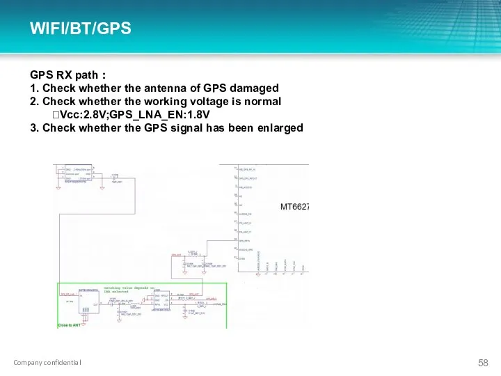
- 58. WIFI/BT/GPS GPS RX path : 1. Check whether the antenna of GPS damaged 2. Check whether
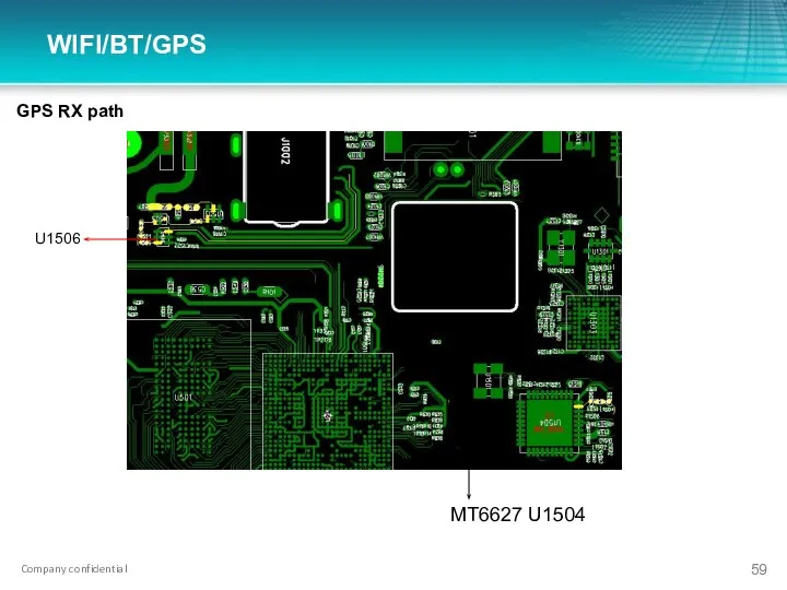
- 59. WIFI/BT/GPS GPS RX path MT6627 U1504 U1506
- 61. Скачать презентацию
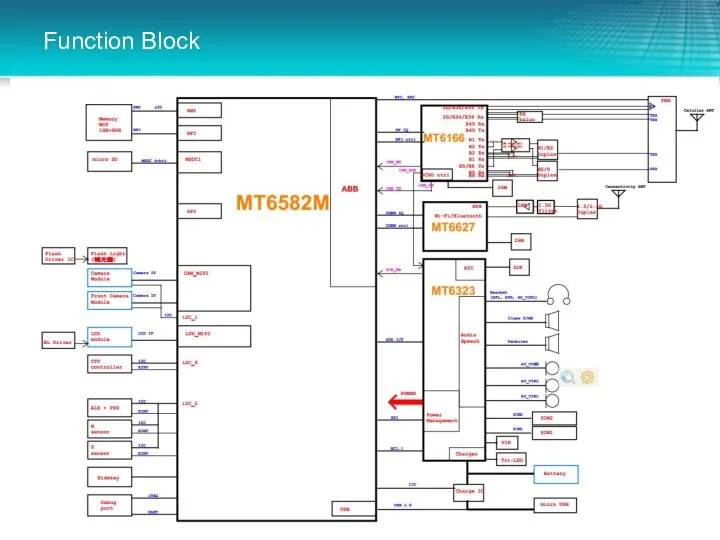
Function Block
Function Block
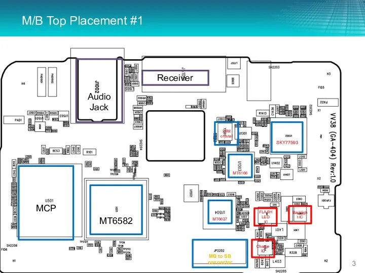
M/B Top Placement #1
MT6582
MCP
Charge IC
Audio Jack
Receiver
SKY77593
MT6166
FLASH
LED
IC
Backlight IC
26M crystal
MT6627
MB to SB
M/B Top Placement #1
MT6582
MCP
Charge IC
Audio Jack
Receiver
SKY77593
MT6166
FLASH
LED
IC
Backlight IC
26M crystal
MT6627
MB to SB
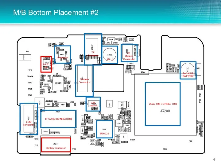
M/B Bottom Placement #2
MT6323
DUAL SIM CONNECTOR
BACK UP BATTERY
Mic 2
TF CARD CONNECTOR
Battery
M/B Bottom Placement #2
MT6323
DUAL SIM CONNECTOR
BACK UP BATTERY
Mic 2
TF CARD CONNECTOR
Battery
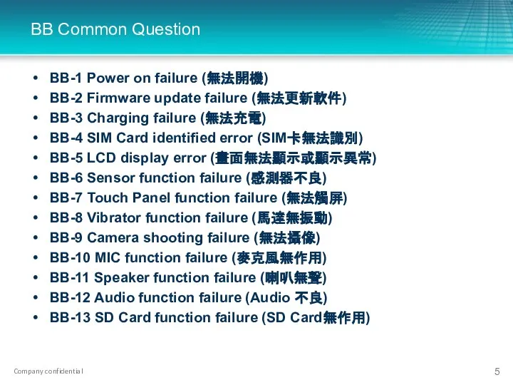
BB Common Question
BB-1 Power on failure (無法開機)
BB-2 Firmware update failure (無法更新軟件)
BB-3
BB Common Question
BB-1 Power on failure (無法開機)
BB-2 Firmware update failure (無法更新軟件)
BB-3
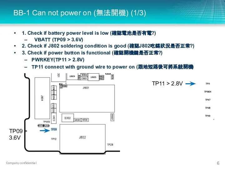
BB-1 Can not power on (無法開機) (1/3)
1. Check if battery power
BB-1 Can not power on (無法開機) (1/3)
1. Check if battery power
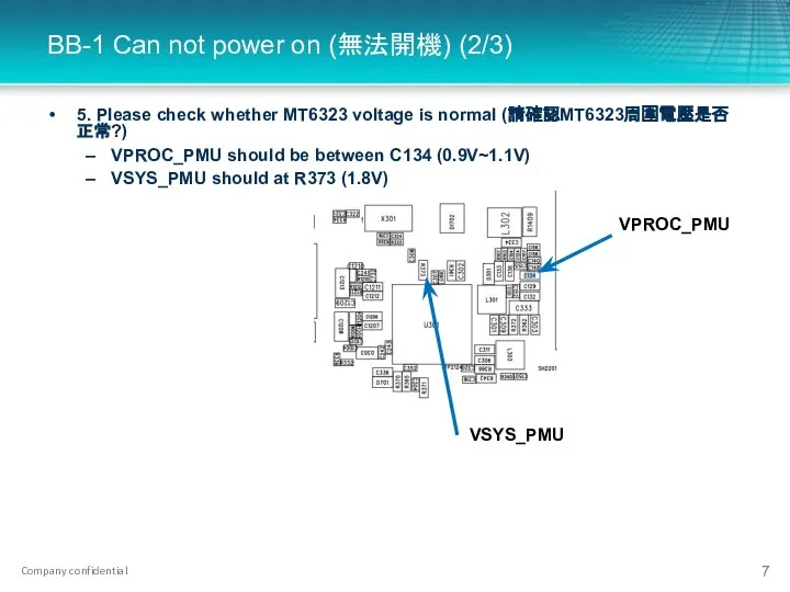
5. Please check whether MT6323 voltage is normal (請確認MT6323周圍電壓是否正常?)
VPROC_PMU should be
5. Please check whether MT6323 voltage is normal (請確認MT6323周圍電壓是否正常?)
VPROC_PMU should be
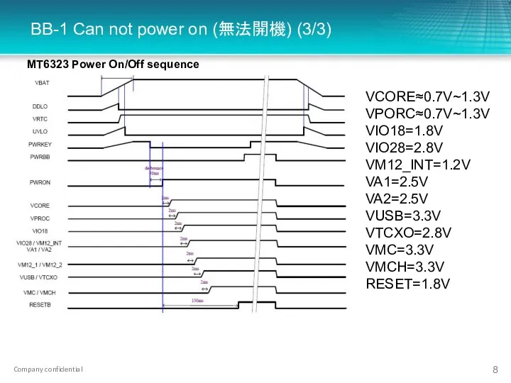
BB-1 Can not power on (無法開機) (3/3)
VCORE≈0.7V~1.3V
VPORC≈0.7V~1.3V
VIO18=1.8V
VIO28=2.8V
VM12_INT=1.2V
VA1=2.5V
VA2=2.5V
VUSB=3.3V
VTCXO=2.8V
VMC=3.3V
VMCH=3.3V
RESET=1.8V
MT6323 Power On/Off sequence
BB-1 Can not power on (無法開機) (3/3)
VCORE≈0.7V~1.3V
VPORC≈0.7V~1.3V
VIO18=1.8V
VIO28=2.8V
VM12_INT=1.2V
VA1=2.5V
VA2=2.5V
VUSB=3.3V
VTCXO=2.8V
VMC=3.3V
VMCH=3.3V
RESET=1.8V
MT6323 Power On/Off sequence
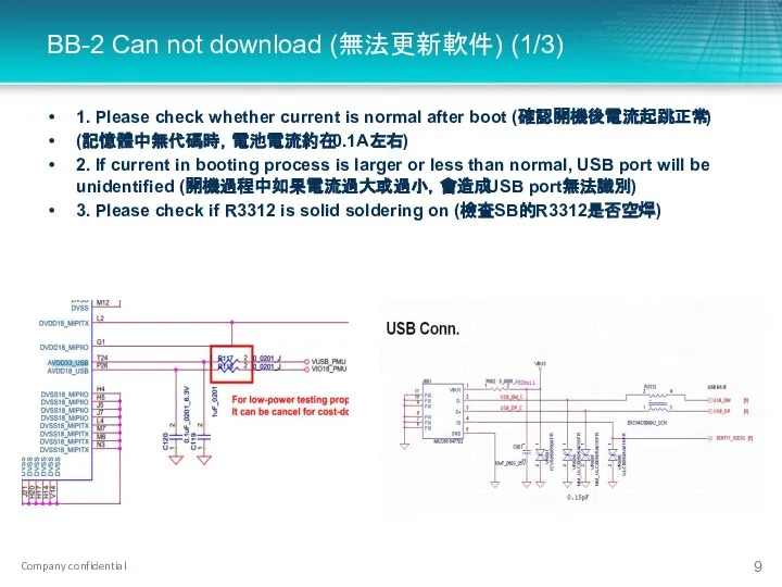
BB-2 Can not download (無法更新軟件) (1/3)
1. Please check whether current is
BB-2 Can not download (無法更新軟件) (1/3)
1. Please check whether current is
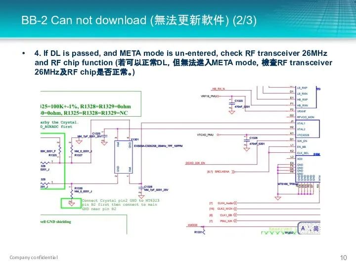
BB-2 Can not download (無法更新軟件) (2/3)
4. If DL is passed, and
BB-2 Can not download (無法更新軟件) (2/3)
4. If DL is passed, and
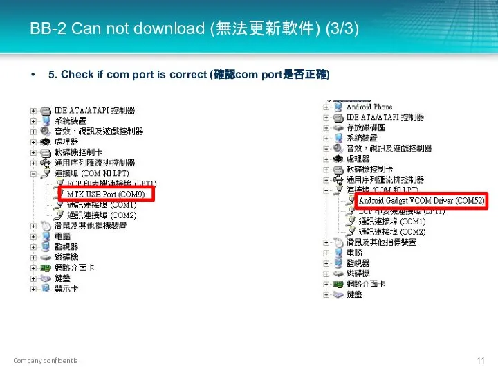
BB-2 Can not download (無法更新軟件) (3/3)
5. Check if com port is
BB-2 Can not download (無法更新軟件) (3/3)
5. Check if com port is
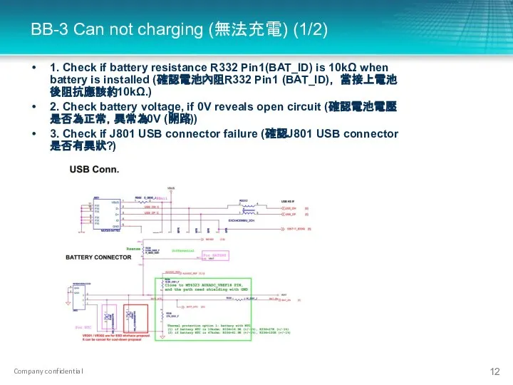
BB-3 Can not charging (無法充電) (1/2)
1. Check if battery resistance R332
BB-3 Can not charging (無法充電) (1/2)
1. Check if battery resistance R332
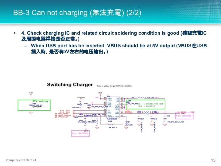
BB-3 Can not charging (無法充電) (2/2)
4. Check charging IC and related
BB-3 Can not charging (無法充電) (2/2)
4. Check charging IC and related
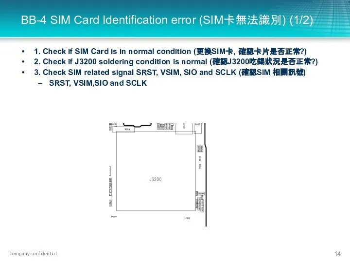
BB-4 SIM Card Identification error (SIM卡無法識別) (1/2)
1. Check if SIM Card
BB-4 SIM Card Identification error (SIM卡無法識別) (1/2)
1. Check if SIM Card
BB-4 SIM Card Identification error (SIM卡無法識別) (2/2)
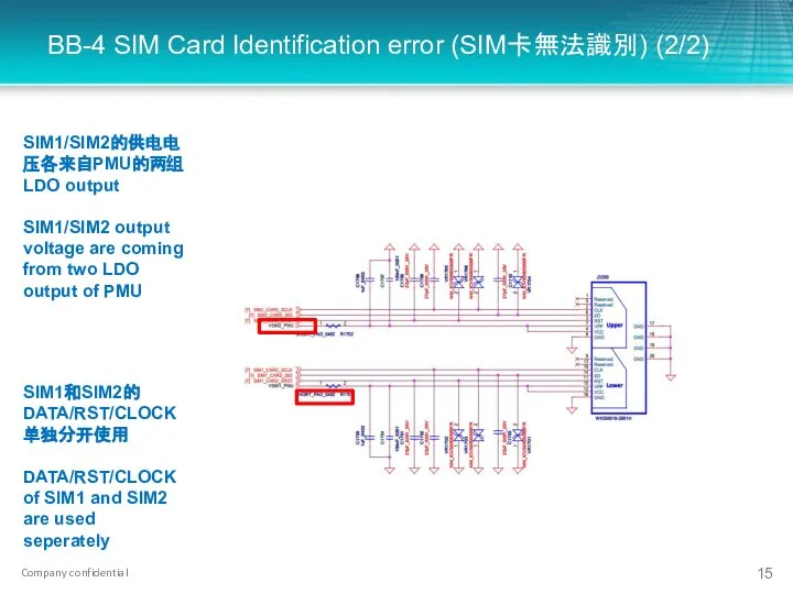
SIM1和SIM2的DATA/RST/CLOCK单独分开使用
DATA/RST/CLOCK of SIM1 and SIM2
BB-4 SIM Card Identification error (SIM卡無法識別) (2/2)
SIM1和SIM2的DATA/RST/CLOCK单独分开使用
DATA/RST/CLOCK of SIM1 and SIM2
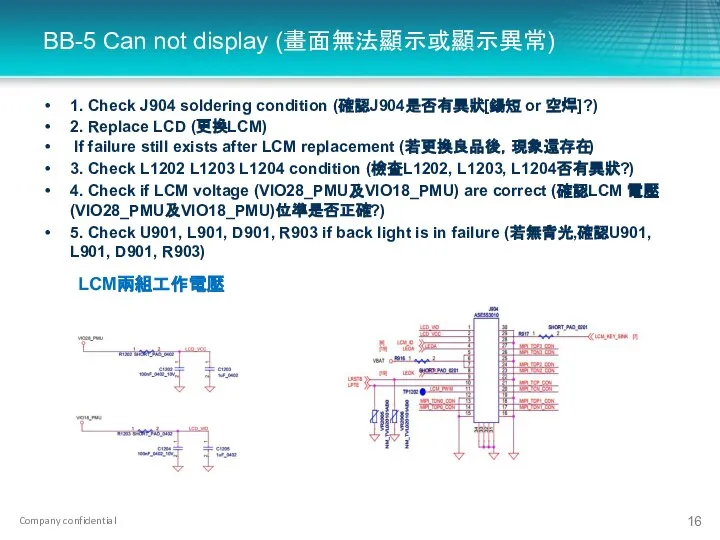
BB-5 Can not display (畫面無法顯示或顯示異常)
1. Check J904 soldering condition (確認J904是否有異狀[鍚短
BB-5 Can not display (畫面無法顯示或顯示異常)
1. Check J904 soldering condition (確認J904是否有異狀[鍚短
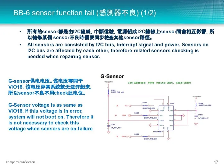
G-sensor供电电压。该电压等同于VIO18,该电压异常系统就无法开起来,所以sensor不良不用check此电位。
G-Sensor voltage is as same as VIO18. if this voltage is
G-sensor供电电压。该电压等同于VIO18,该电压异常系统就无法开起来,所以sensor不良不用check此电位。
G-Sensor voltage is as same as VIO18. if this voltage is
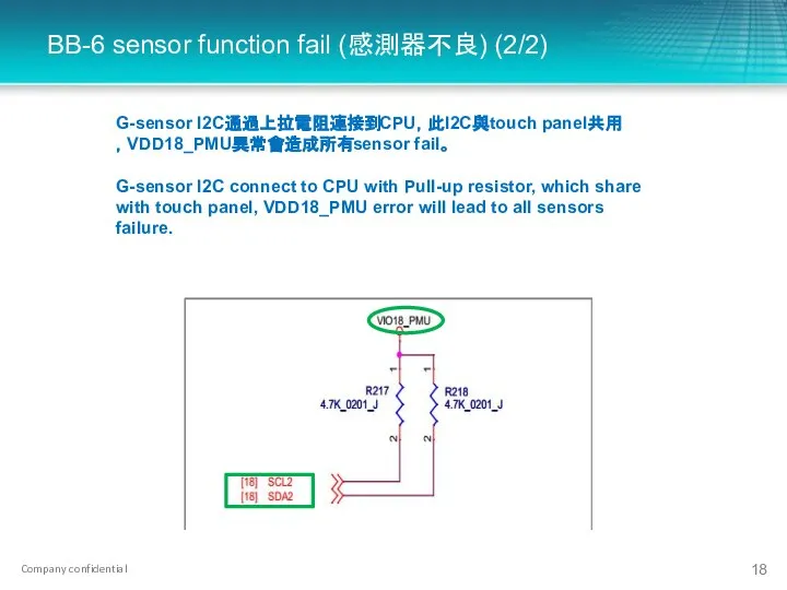
BB-6 sensor function fail (感測器不良) (2/2)
G-sensor I2C通過上拉電阻連接到CPU,此I2C與touch panel共用,VDD18_PMU異常會造成所有sensor fail。
G-sensor I2C connect
BB-6 sensor function fail (感測器不良) (2/2)
G-sensor I2C通過上拉電阻連接到CPU,此I2C與touch panel共用,VDD18_PMU異常會造成所有sensor fail。
G-sensor I2C connect
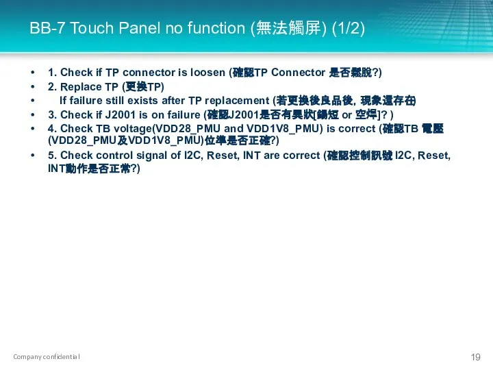
BB-7 Touch Panel no function (無法觸屏) (1/2)
1. Check if TP connector
BB-7 Touch Panel no function (無法觸屏) (1/2)
1. Check if TP connector
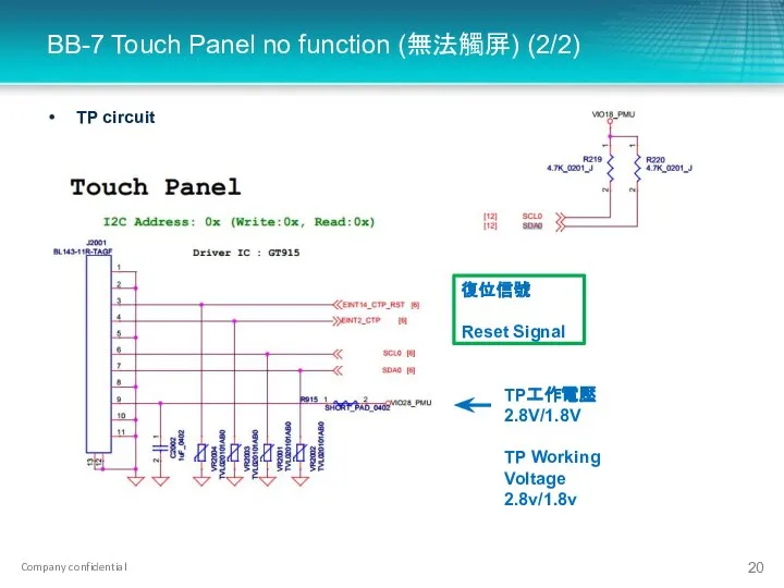
BB-7 Touch Panel no function (無法觸屏) (2/2)
TP circuit
TP工作電壓2.8V/1.8V
TP Working Voltage 2.8v/1.8v
BB-7 Touch Panel no function (無法觸屏) (2/2)
TP circuit
TP工作電壓2.8V/1.8V
TP Working Voltage 2.8v/1.8v
BB-8 Vibrator no function (馬達無振動)
1. Check if motor is in normal
BB-8 Vibrator no function (馬達無振動)
1. Check if motor is in normal
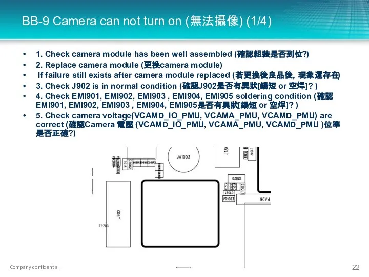
BB-9 Camera can not turn on (無法攝像) (1/4)
1. Check camera module
BB-9 Camera can not turn on (無法攝像) (1/4)
1. Check camera module
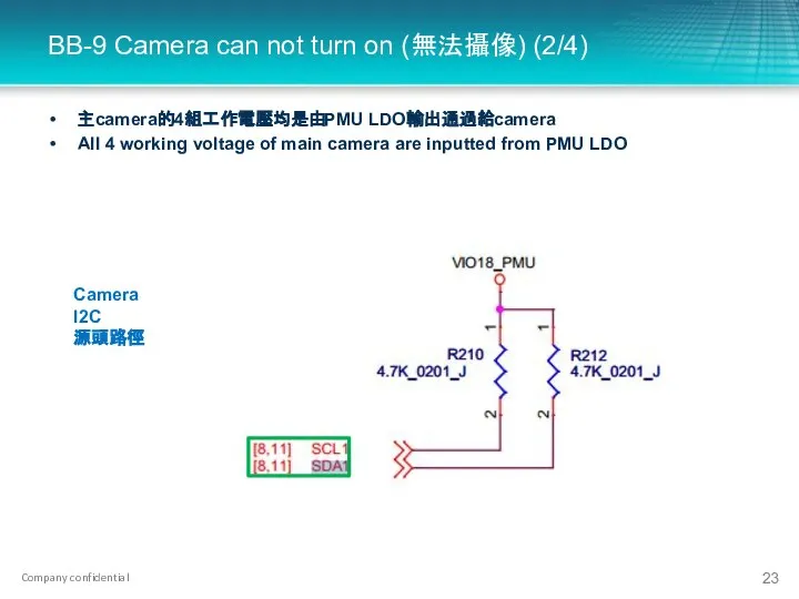
BB-9 Camera can not turn on (無法攝像) (2/4)
主camera的4組工作電壓均是由PMU LDO輸出通過給camera
All 4 working
BB-9 Camera can not turn on (無法攝像) (2/4)
主camera的4組工作電壓均是由PMU LDO輸出通過給camera
All 4 working
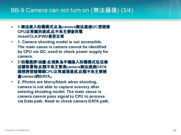
BB-9 Camera can not turn on (無法攝像) (3/4)
1:無法進入拍攝模式,此為camera無法通過I2C信號被CPU正常識別造成,此不良主要查供電/reset/CLK/PWD是否正常
1. Camera shooting model
BB-9 Camera can not turn on (無法攝像) (3/4)
1:無法進入拍攝模式,此為camera無法通過I2C信號被CPU正常識別造成,此不良主要查供電/reset/CLK/PWD是否正常
1. Camera shooting model
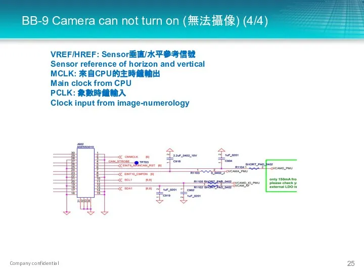
BB-9 Camera can not turn on (無法攝像) (4/4)
VREF/HREF: Sensor垂直/水平參考信號
Sensor reference of
BB-9 Camera can not turn on (無法攝像) (4/4)
VREF/HREF: Sensor垂直/水平參考信號
Sensor reference of
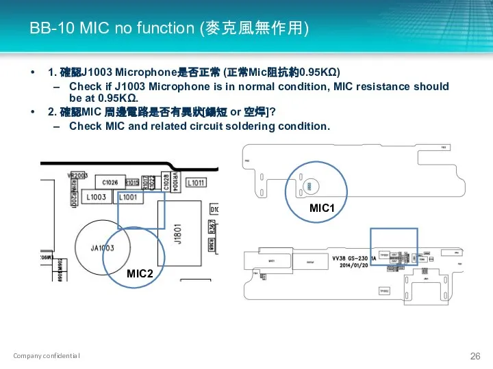
BB-10 MIC no function (麥克風無作用)
1. 確認J1003 Microphone是否正常 (正常Mic阻抗約0.95KΩ)
Check if J1003 Microphone
BB-10 MIC no function (麥克風無作用)
1. 確認J1003 Microphone是否正常 (正常Mic阻抗約0.95KΩ)
Check if J1003 Microphone
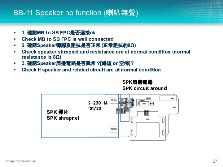
BB-11 Speaker no function (喇叭無聲)
1. 確認MB to SB FPC是否連接ok
Check MB to
BB-11 Speaker no function (喇叭無聲)
1. 確認MB to SB FPC是否連接ok
Check MB to
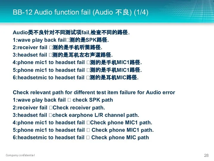
BB-12 Audio function fail (Audio 不良) (1/4)
Audio类不良针对不同测试项fail,检查不同的路径.
1:wave play back fail?测的是SPK路径.
2:receiver fail
BB-12 Audio function fail (Audio 不良) (1/4)
Audio类不良针对不同测试项fail,检查不同的路径.
1:wave play back fail?测的是SPK路径.
2:receiver fail
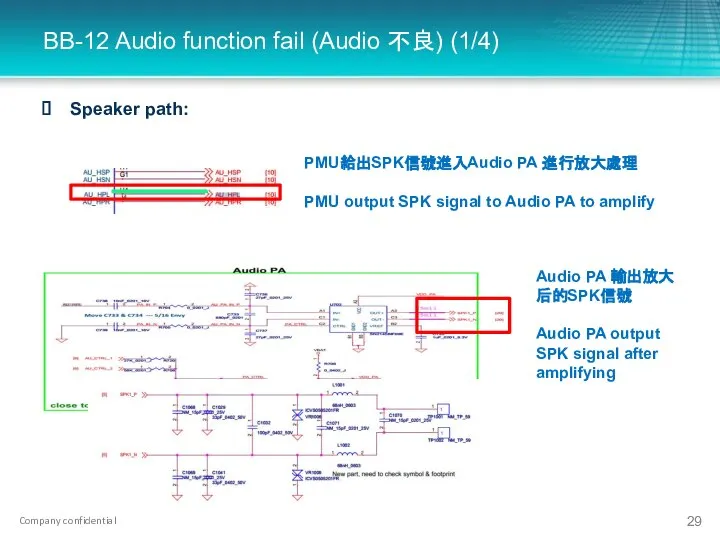
BB-12 Audio function fail (Audio 不良) (1/4)
Speaker path:
PMU給出SPK信號進入Audio PA 進行放大處理
PMU output
BB-12 Audio function fail (Audio 不良) (1/4)
Speaker path:
PMU給出SPK信號進入Audio PA 進行放大處理
PMU output
BB-12 Audio function fail (Audio 不良) (2/4)
Receiver path:
Phone MIC path
PMU輸出音頻信號
PMU output
BB-12 Audio function fail (Audio 不良) (2/4)
Receiver path:
Phone MIC path
PMU輸出音頻信號
PMU output
BB-12 Audio function fail (Audio 不良) (3/4)
耳機左右聲道電路: Earphone L/R channel circuit
PMU輸出耳機音頻信號
PMU
BB-12 Audio function fail (Audio 不良) (3/4)
耳機左右聲道電路: Earphone L/R channel circuit
PMU輸出耳機音頻信號
PMU
BB-12 Audio function fail (Audio 不良) (4/4)
耳機MIC電路 Earphone MIC Circuit:
為耳機MIC提供偏置電壓
Provide bias
BB-12 Audio function fail (Audio 不良) (4/4)
耳機MIC電路 Earphone MIC Circuit:
為耳機MIC提供偏置電壓
Provide bias
BB-13 SD Card no function (SD Card無作用)
SD card 偵測信號
SD card signal
BB-13 SD Card no function (SD Card無作用)
SD card 偵測信號
SD card signal
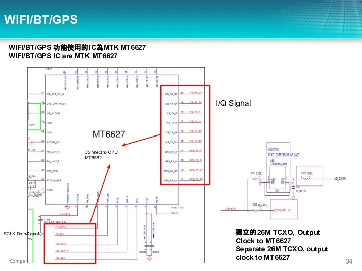
WIFI/BT/GPS
I/Q Signal
SCLK,DataSignal
Connect to CPU MT6582
獨立的26M TCXO,Output Clock to MT6627
Separate 26M TCXO,
WIFI/BT/GPS
I/Q Signal
SCLK,DataSignal
Connect to CPU MT6582
獨立的26M TCXO,Output Clock to MT6627
Separate 26M TCXO,
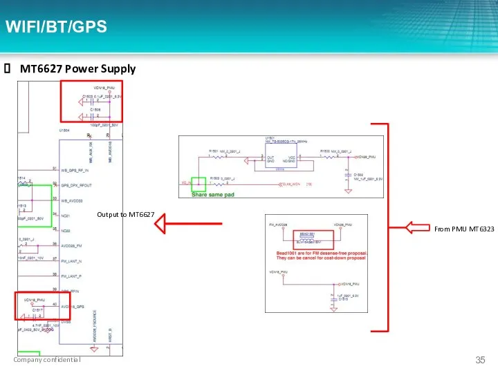
MT6627 Power Supply
WIFI/BT/GPS
From PMU MT6323
Output to MT6627
MT6627 Power Supply
WIFI/BT/GPS
From PMU MT6323
Output to MT6627
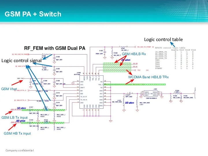
GSM PA + Switch
GSM Vbat
GSM LB Tx input
GSM HB Tx input
WCDMA
GSM PA + Switch
GSM Vbat
GSM LB Tx input
GSM HB Tx input
WCDMA
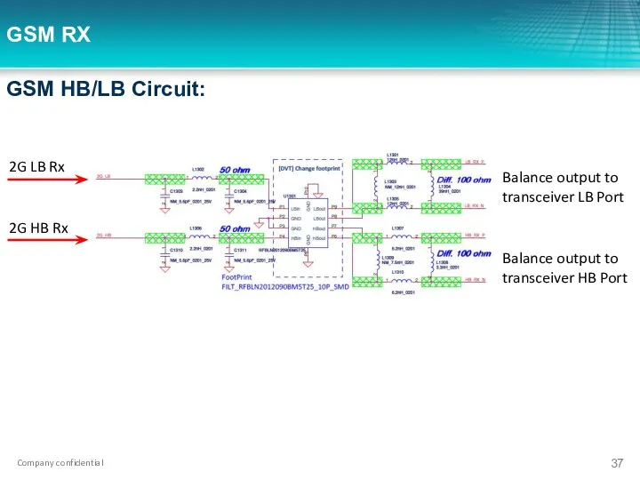
GSM RX
GSM HB/LB Circuit:
2G LB Rx
2G HB Rx
Balance output to transceiver
GSM RX
GSM HB/LB Circuit:
2G LB Rx
2G HB Rx
Balance output to transceiver
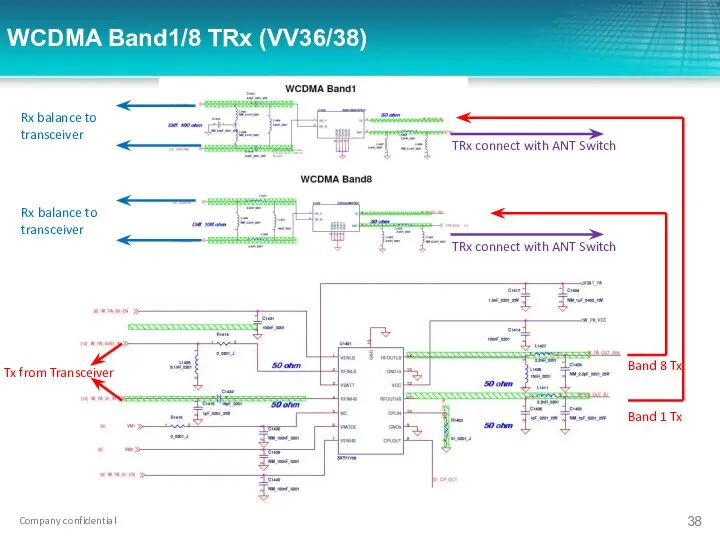
WCDMA Band1/8 TRx (VV36/38)
Tx from Transceiver
Band 8 Tx
Rx balance to transceiver
TRx
WCDMA Band1/8 TRx (VV36/38)
Tx from Transceiver
Band 8 Tx
Rx balance to transceiver
TRx
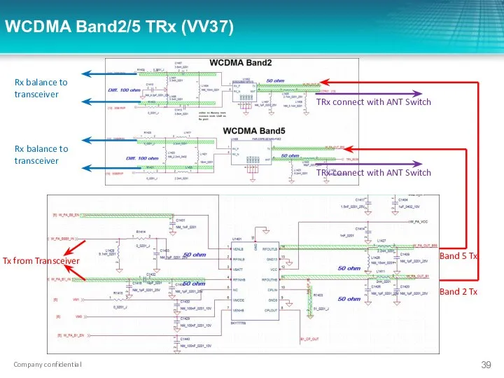
WCDMA Band2/5 TRx (VV37)
Tx from Transceiver
Band 5 Tx
Rx balance to transceiver
TRx
WCDMA Band2/5 TRx (VV37)
Tx from Transceiver
Band 5 Tx
Rx balance to transceiver
TRx
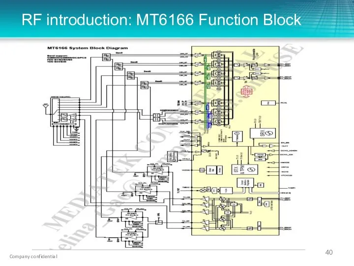
RF introduction: MT6166 Function Block
RF introduction: MT6166 Function Block
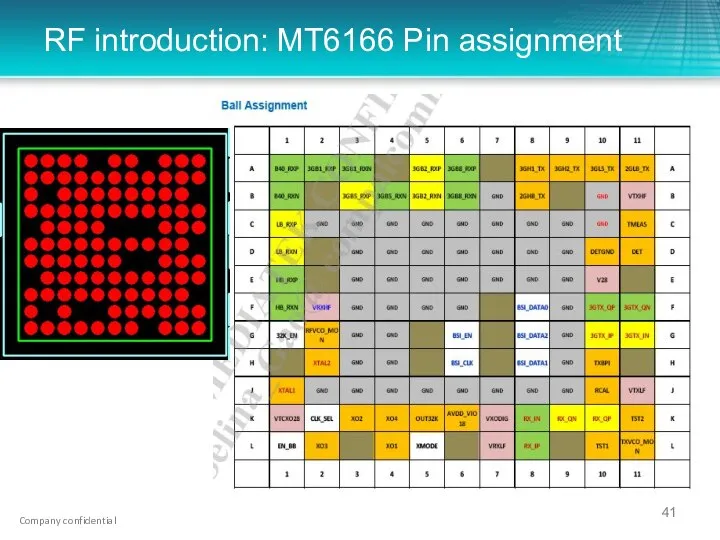
RF introduction: MT6166 Pin assignment
RF introduction: MT6166 Pin assignment
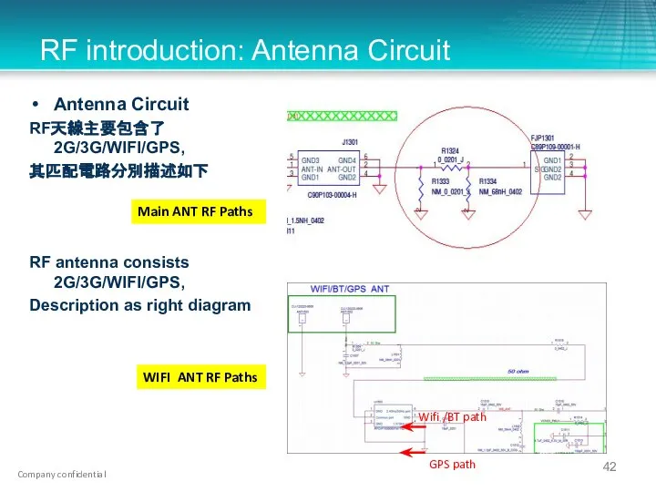
RF introduction: Antenna Circuit
Antenna Circuit
RF天線主要包含了2G/3G/WIFI/GPS,
其匹配電路分別描述如下
RF antenna consists 2G/3G/WIFI/GPS,
Description as
RF introduction: Antenna Circuit
Antenna Circuit
RF天線主要包含了2G/3G/WIFI/GPS,
其匹配電路分別描述如下
RF antenna consists 2G/3G/WIFI/GPS,
Description as
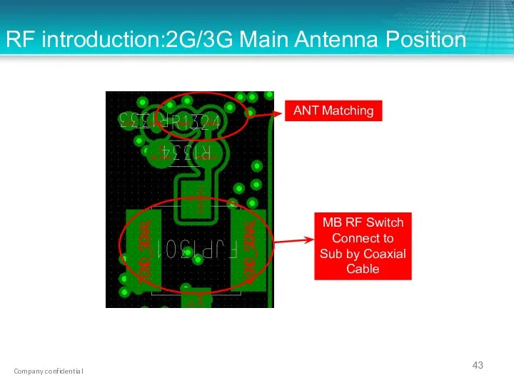
RF introduction:2G/3G Main Antenna Position
RF introduction:2G/3G Main Antenna Position
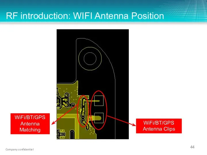
RF introduction: WIFI Antenna Position
RF introduction: WIFI Antenna Position
RF common issue
RF-1:Network function error
RF-2:GSM problem
RF-3:WCDMA problem
RF-4:GSM/WCDMA Rx error
RF-5:WIFI problem
RF common issue
RF-1:Network function error
RF-2:GSM problem
RF-3:WCDMA problem
RF-4:GSM/WCDMA Rx error
RF-5:WIFI problem
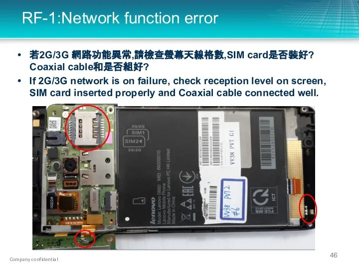
RF-1:Network function error
若2G/3G 網路功能異常,請檢查螢幕天線格數,SIM card是否裝好? Coaxial cable和是否組好?
If 2G/3G network is on
RF-1:Network function error
若2G/3G 網路功能異常,請檢查螢幕天線格數,SIM card是否裝好? Coaxial cable和是否組好?
If 2G/3G network is on
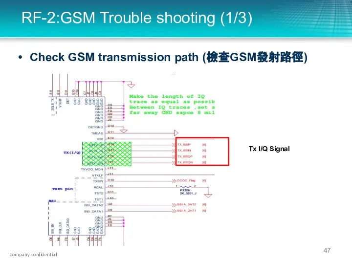
RF-2:GSM Trouble shooting (1/3)
Check GSM transmission path (檢查GSM發射路徑)
Tx I/Q Signal
RF-2:GSM Trouble shooting (1/3)
Check GSM transmission path (檢查GSM發射路徑)
Tx I/Q Signal
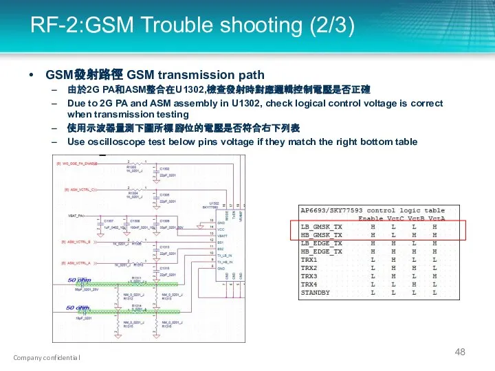
RF-2:GSM Trouble shooting (2/3)
GSM發射路徑 GSM transmission path
由於2G PA和ASM整合在U1302,檢查發射時對應邏輯控制電壓是否正確
Due to 2G
RF-2:GSM Trouble shooting (2/3)
GSM發射路徑 GSM transmission path
由於2G PA和ASM整合在U1302,檢查發射時對應邏輯控制電壓是否正確
Due to 2G
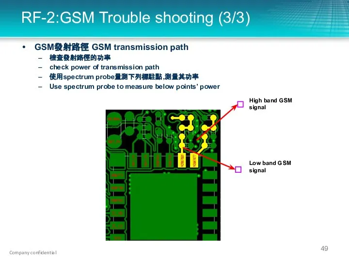
RF-2:GSM Trouble shooting (3/3)
GSM發射路徑 GSM transmission path
檢查發射路徑的功率
check power of transmission path
使用spectrum
RF-2:GSM Trouble shooting (3/3)
GSM發射路徑 GSM transmission path
檢查發射路徑的功率
check power of transmission path
使用spectrum
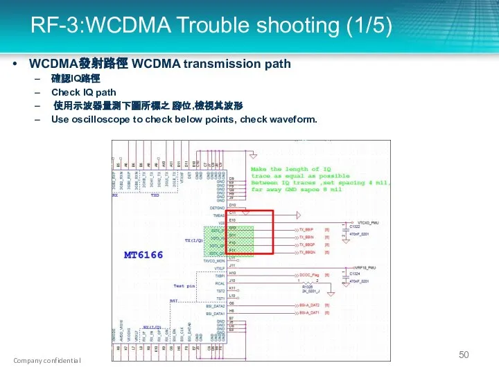
RF-3:WCDMA Trouble shooting (1/5)
WCDMA發射路徑 WCDMA transmission path
確認IQ路徑
Check IQ path
使用示波器量測下圖所標之腳位,檢視其波形
Use oscilloscope
RF-3:WCDMA Trouble shooting (1/5)
WCDMA發射路徑 WCDMA transmission path
確認IQ路徑
Check IQ path
使用示波器量測下圖所標之腳位,檢視其波形
Use oscilloscope
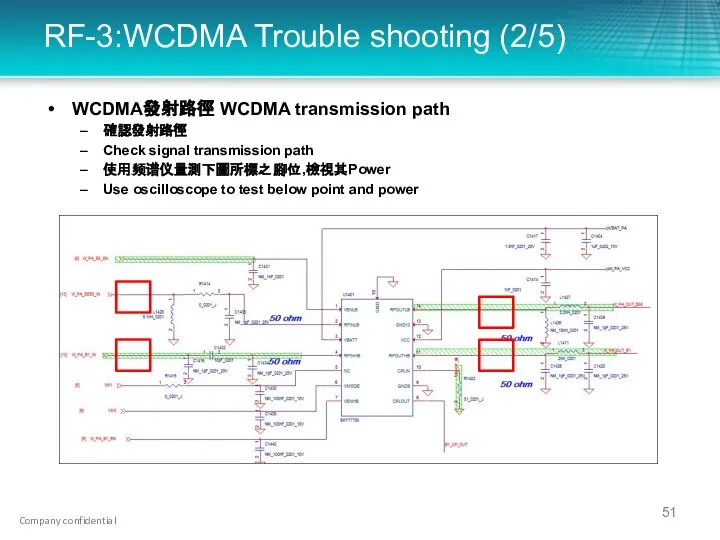
RF-3:WCDMA Trouble shooting (2/5)
WCDMA發射路徑 WCDMA transmission path
確認發射路徑
Check signal transmission path
使用频谱仪量測下圖所標之腳位,檢視其Power
Use oscilloscope
RF-3:WCDMA Trouble shooting (2/5)
WCDMA發射路徑 WCDMA transmission path
確認發射路徑
Check signal transmission path
使用频谱仪量測下圖所標之腳位,檢視其Power
Use oscilloscope
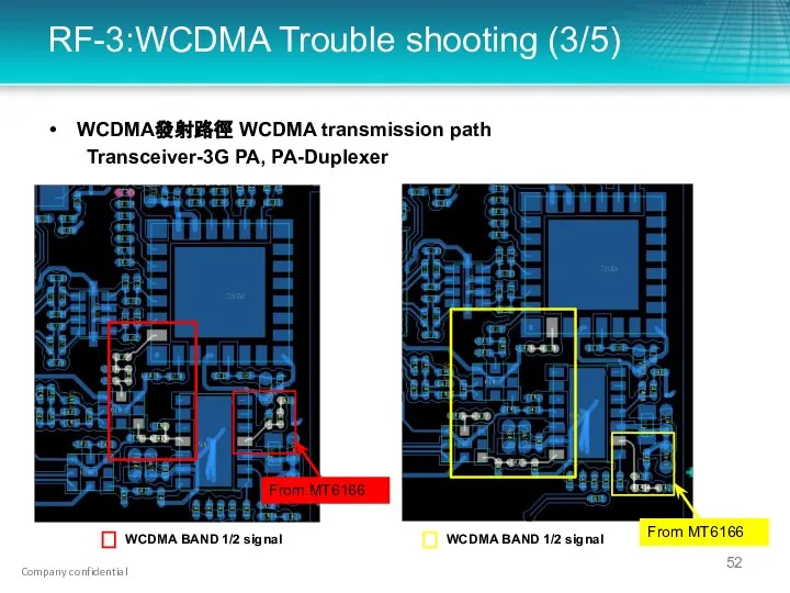
RF-3:WCDMA Trouble shooting (3/5)
WCDMA發射路徑 WCDMA transmission path
Transceiver-3G PA, PA-Duplexer
From MT6166
WCDMA BAND
RF-3:WCDMA Trouble shooting (3/5)
WCDMA發射路徑 WCDMA transmission path
Transceiver-3G PA, PA-Duplexer
From MT6166
WCDMA BAND
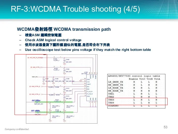
RF-3:WCDMA Trouble shooting (4/5)
WCDMA發射路徑 WCDMA transmission path
檢查ASM 邏輯控制電壓
Check ASM logical
RF-3:WCDMA Trouble shooting (4/5)
WCDMA發射路徑 WCDMA transmission path
檢查ASM 邏輯控制電壓
Check ASM logical
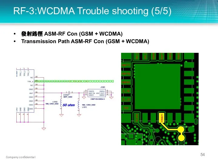
RF-3:WCDMA Trouble shooting (5/5)
GSM PA+ASM
發射路徑 ASM-RF Con (GSM + WCDMA)
Transmission Path
RF-3:WCDMA Trouble shooting (5/5)
GSM PA+ASM
發射路徑 ASM-RF Con (GSM + WCDMA)
Transmission Path
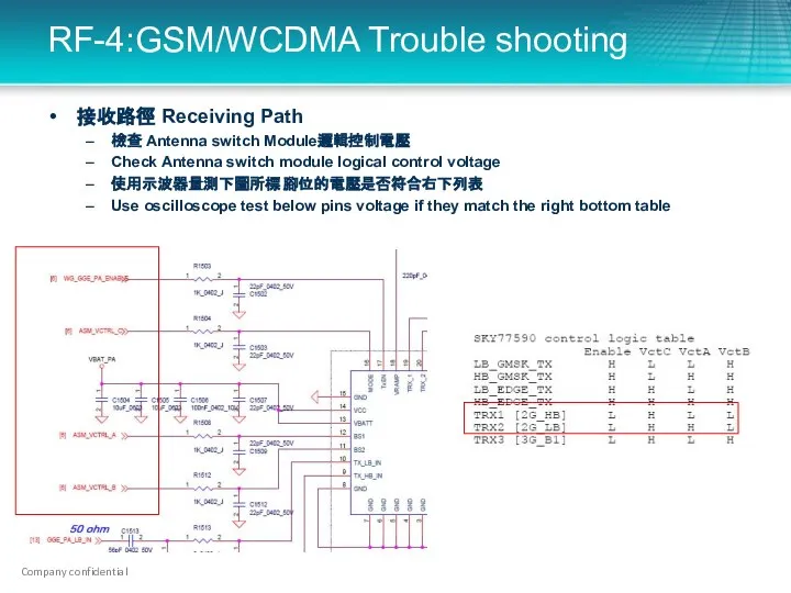
RF-4:GSM/WCDMA Trouble shooting
接收路徑 Receiving Path
檢查 Antenna switch Module邏輯控制電壓
Check Antenna switch module
RF-4:GSM/WCDMA Trouble shooting
接收路徑 Receiving Path
檢查 Antenna switch Module邏輯控制電壓
Check Antenna switch module
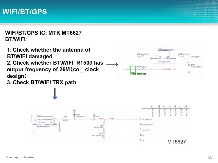
WIFI/BT/GPS
WIFI/BT/GPS IC: MTK MT6627
BT/WIFI:
1. Check whether the antenna of BT\WIFI
WIFI/BT/GPS
WIFI/BT/GPS IC: MTK MT6627
BT/WIFI:
1. Check whether the antenna of BT\WIFI
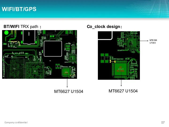
WIFI/BT/GPS
BT/WIFI TRX path :
MT6627 U1504
MT6627 U1504
MT6166 U1303
Co_clock design:
WIFI/BT/GPS
BT/WIFI TRX path :
MT6627 U1504
MT6627 U1504
MT6166 U1303
Co_clock design:
WIFI/BT/GPS
GPS RX path :
1. Check whether the antenna of GPS damaged
2.
WIFI/BT/GPS
GPS RX path :
1. Check whether the antenna of GPS damaged
2.
WIFI/BT/GPS
GPS RX path
MT6627 U1504
U1506
WIFI/BT/GPS
GPS RX path
MT6627 U1504
U1506
 «…современный урок должен стать уроком творческой дружбы учителя и ученика.» (Куманев А.А.). Примерная структура каждого типа урока по ФГОС
 Специфические методы и этапы статистического исследования
 роутеры тетрадь
 Культура во второй половине XX – начала XXI в. (Новейшая история 9 класс)
 Виды и закономерности изнашивания
 ЕВРОПЕЙСКАЯ ИНТЕГРАЦИЯ Научный руководитель Писарев В.М.
  Муниципальное казённое дошкольное образовательное учреждение «Детский сад № 1» «Современные здоровьесберегающие технологии»
 Макроэкономические показатели (система национальных счетов) ВВП и его структура
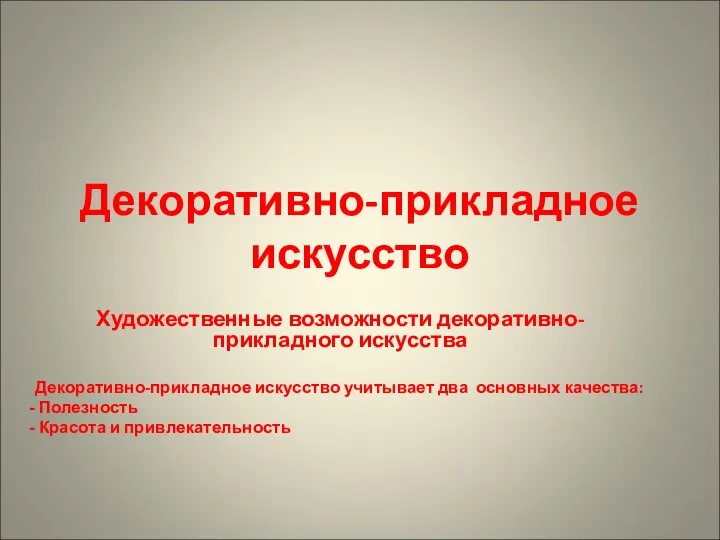 Декоративно-прикладное искусство
 Проекционное черчение. Проецирование на несколько проекций
 Подготовка соревнований
 Страницы биографии поэта Николая Алексеевича Некрасова (1821-1877)
 Презентация на тему "Психолого-педагогическая характеристика детей, обучающихся по специальной (коррекционной) программе школ
 Сметные цены в строительстве
 Сказочно – былинный жанр в живописи
 Любимый ученик Христа Иоанн Богослов
 Лекция 9. Ислам
 Международные экономические отношения. Права человека и международные отношения
 понятие риска. биологические,химические, физические факторы риска Выполнили: студенты ФТД-1 группы Т-116 Федина Юля и Цьопа Даша _
 Теоретические основы процесса оцифровки
 Сфинкс. Плато Гизе
 Урок-по-духовному-краеведению-Что-такое-религиозная-культура
 Языковой клуб. Группы языкового самообразования от Молодежного Совета ФГБУ “НИИ ЦПК им Гагарина” и МЦ “Галактика”
 《发展汉语(第二版)初级综合(Ⅰ)》第13课+课件
 Московский Кремль
 Лечебная физкультура при нарушениях осанки
 Презентация Анализ международного контекста модернизации высшего образования
  Умножение десятичных дробей - презентация по Алгебре