- Simulation with Conditions

Содержание
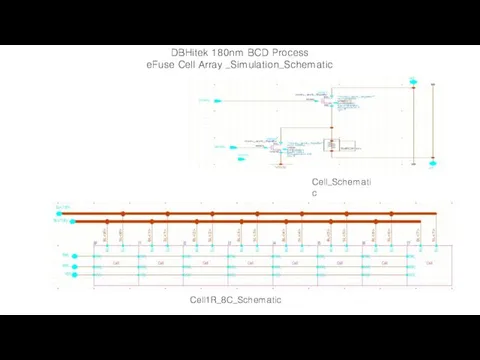
- 2. DBHitek 180nm BCD Process eFuse Cell Array _Simulation_Schematic Cell_Schematic Cell1R_8C_Schematic
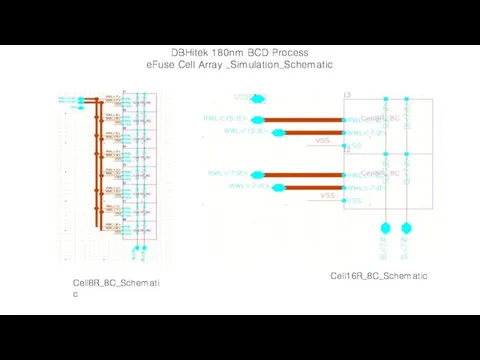
- 3. DBHitek 180nm BCD Process eFuse Cell Array _Simulation_Schematic Cell16R_8C_Schematic Cell8R_8C_Schematic
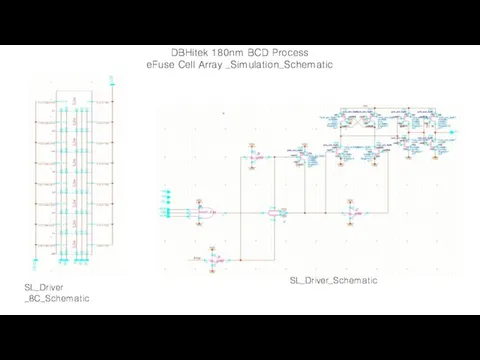
- 4. DBHitek 180nm BCD Process eFuse Cell Array _Simulation_Schematic SL_Driver _8C_Schematic SL_Driver_Schematic
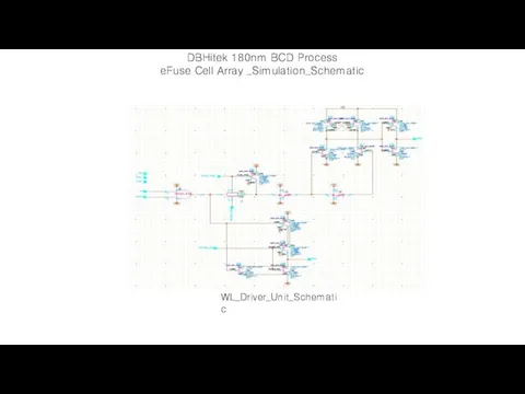
- 5. DBHitek 180nm BCD Process eFuse Cell Array _Simulation_Schematic WL_Driver_Unit_Schematic
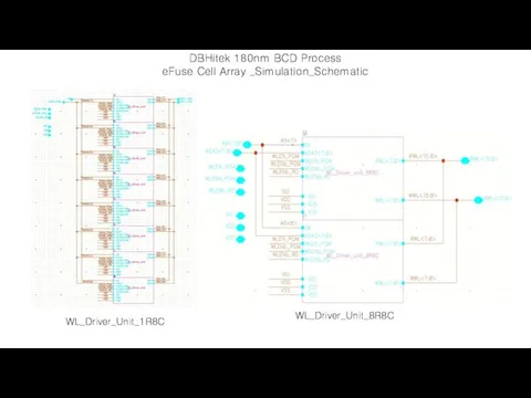
- 6. DBHitek 180nm BCD Process eFuse Cell Array _Simulation_Schematic WL_Driver_Unit_8R8C WL_Driver_Unit_1R8C
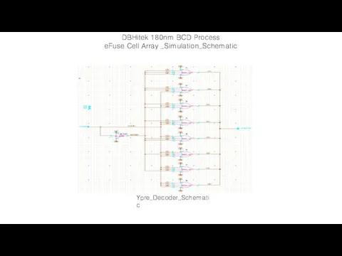
- 7. DBHitek 180nm BCD Process eFuse Cell Array _Simulation_Schematic Ypre_Decoder_Schematic
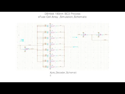
- 8. DBHitek 180nm BCD Process eFuse Cell Array _Simulation_Schematic Xpre_Decoder_Schematic
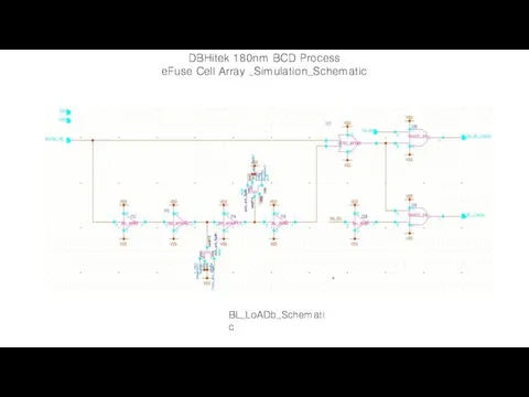
- 9. DBHitek 180nm BCD Process eFuse Cell Array _Simulation_Schematic BL_LoADb_Schematic
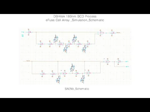
- 10. DBHitek 180nm BCD Process eFuse Cell Array _Simulation_Schematic SAENb_Schematic
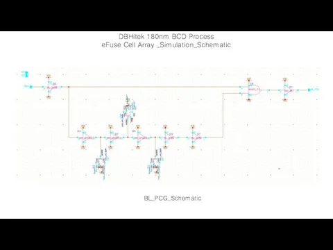
- 11. DBHitek 180nm BCD Process eFuse Cell Array _Simulation_Schematic BL_PCG_Schematic
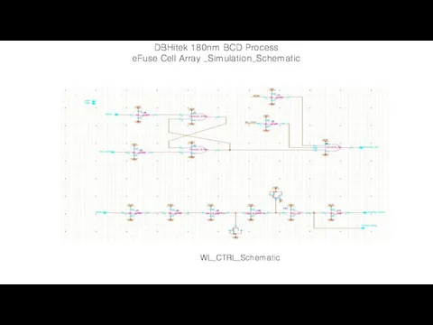
- 12. DBHitek 180nm BCD Process eFuse Cell Array _Simulation_Schematic WL_CTRL_Schematic
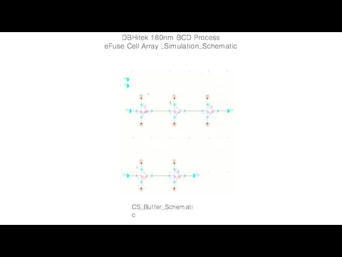
- 13. DBHitek 180nm BCD Process eFuse Cell Array _Simulation_Schematic CS_Buffer_Schematic
- 14. BL_SA_CTRL_Schematic DBHitek 180nm BCD Process eFuse Cell Array _Simulation_Schematic
- 15. Control_Logic_Schematic DBHitek 180nm BCD Process eFuse Cell Array _Simulation_Schematic
- 16. Core_Schematic DBHitek 180nm BCD Process eFuse Cell Array _Simulation_Schematic
- 17. Top_Schematic DBHitek 180nm BCD Process eFuse Cell Array _Simulation_Schematic
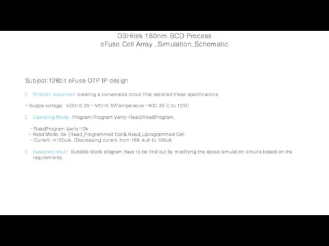
- 18. DBHitek 180nm BCD Process eFuse Cell Array _Simulation_Schematic Subject:128bit eFuse OTP IP design Problem statement:creating a
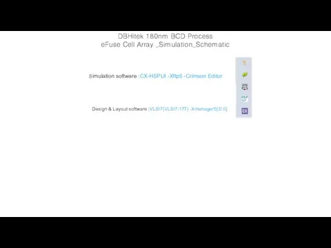
- 19. DBHitek 180nm BCD Process eFuse Cell Array _Simulation_Schematic Simulation software :CX-HSPUI -Xftp5 -Crimson Editor Design &
- 21. Скачать презентацию
DBHitek 180nm BCD Process
eFuse Cell Array _Simulation_Schematic
Cell_Schematic
Cell1R_8C_Schematic
DBHitek 180nm BCD Process
eFuse Cell Array _Simulation_Schematic
Cell_Schematic
Cell1R_8C_Schematic
DBHitek 180nm BCD Process
eFuse Cell Array _Simulation_Schematic
Cell16R_8C_Schematic
Cell8R_8C_Schematic
DBHitek 180nm BCD Process
eFuse Cell Array _Simulation_Schematic
Cell16R_8C_Schematic
Cell8R_8C_Schematic
DBHitek 180nm BCD Process
eFuse Cell Array _Simulation_Schematic
SL_Driver _8C_Schematic
SL_Driver_Schematic
DBHitek 180nm BCD Process
eFuse Cell Array _Simulation_Schematic
SL_Driver _8C_Schematic
SL_Driver_Schematic
DBHitek 180nm BCD Process
eFuse Cell Array _Simulation_Schematic
WL_Driver_Unit_Schematic
DBHitek 180nm BCD Process
eFuse Cell Array _Simulation_Schematic
WL_Driver_Unit_Schematic
DBHitek 180nm BCD Process
eFuse Cell Array _Simulation_Schematic
WL_Driver_Unit_8R8C
WL_Driver_Unit_1R8C
DBHitek 180nm BCD Process
eFuse Cell Array _Simulation_Schematic
WL_Driver_Unit_8R8C
WL_Driver_Unit_1R8C
DBHitek 180nm BCD Process
eFuse Cell Array _Simulation_Schematic
Ypre_Decoder_Schematic
DBHitek 180nm BCD Process
eFuse Cell Array _Simulation_Schematic
Ypre_Decoder_Schematic
DBHitek 180nm BCD Process
eFuse Cell Array _Simulation_Schematic
Xpre_Decoder_Schematic
DBHitek 180nm BCD Process
eFuse Cell Array _Simulation_Schematic
Xpre_Decoder_Schematic
DBHitek 180nm BCD Process
eFuse Cell Array _Simulation_Schematic
BL_LoADb_Schematic
DBHitek 180nm BCD Process
eFuse Cell Array _Simulation_Schematic
BL_LoADb_Schematic
DBHitek 180nm BCD Process
eFuse Cell Array _Simulation_Schematic
SAENb_Schematic
DBHitek 180nm BCD Process
eFuse Cell Array _Simulation_Schematic
SAENb_Schematic
DBHitek 180nm BCD Process
eFuse Cell Array _Simulation_Schematic
BL_PCG_Schematic
DBHitek 180nm BCD Process
eFuse Cell Array _Simulation_Schematic
BL_PCG_Schematic
DBHitek 180nm BCD Process
eFuse Cell Array _Simulation_Schematic
WL_CTRL_Schematic
DBHitek 180nm BCD Process
eFuse Cell Array _Simulation_Schematic
WL_CTRL_Schematic
DBHitek 180nm BCD Process
eFuse Cell Array _Simulation_Schematic
CS_Buffer_Schematic
DBHitek 180nm BCD Process
eFuse Cell Array _Simulation_Schematic
CS_Buffer_Schematic
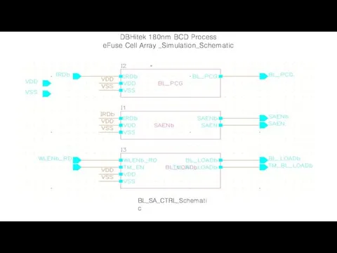
BL_SA_CTRL_Schematic
DBHitek 180nm BCD Process
eFuse Cell Array _Simulation_Schematic
BL_SA_CTRL_Schematic
DBHitek 180nm BCD Process
eFuse Cell Array _Simulation_Schematic
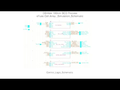
Control_Logic_Schematic
DBHitek 180nm BCD Process
eFuse Cell Array _Simulation_Schematic
Control_Logic_Schematic
DBHitek 180nm BCD Process
eFuse Cell Array _Simulation_Schematic
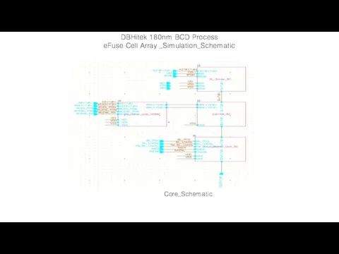
Core_Schematic
DBHitek 180nm BCD Process
eFuse Cell Array _Simulation_Schematic
Core_Schematic
DBHitek 180nm BCD Process
eFuse Cell Array _Simulation_Schematic
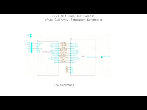
Top_Schematic
DBHitek 180nm BCD Process
eFuse Cell Array _Simulation_Schematic
Top_Schematic
DBHitek 180nm BCD Process
eFuse Cell Array _Simulation_Schematic
DBHitek 180nm BCD Process
eFuse Cell Array _Simulation_Schematic
Subject:128bit eFuse OTP IP design
DBHitek 180nm BCD Process
eFuse Cell Array _Simulation_Schematic
Subject:128bit eFuse OTP IP design
DBHitek 180nm BCD Process
eFuse Cell Array _Simulation_Schematic
Simulation software :CX-HSPUI -Xftp5 -Crimson
DBHitek 180nm BCD Process
eFuse Cell Array _Simulation_Schematic
Simulation software :CX-HSPUI -Xftp5 -Crimson
 История Смоленской Божией Матери Одигитрии
 С Днем освобождения Донбасса!
 Конструктивные схемы зданий и сооружений. Лекция 1
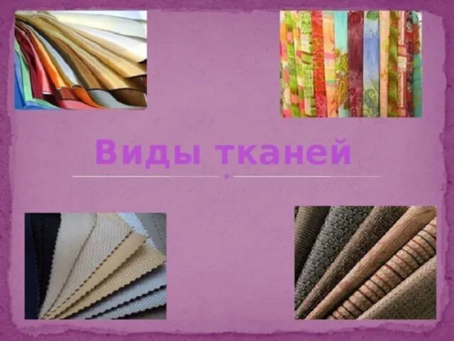 Виды тканей
 20141112_mkhk
 Продукция компании Rombica. Потребительская электроника
 Выпрямитель
 Задание для групп КПИ
 Апокалипсис
 защита — 2003
 Лучшие спортсмены нашей школы
 ПРЕЗЕНТАЦИЯ ДОМАШНИЕ ПТИЦЫ
 Волонтеры здорового образа жизни Психогигиена. Выгорание в сфере волонтёрства
 Пропускная способность ПР пунктов
 Библейский цикл (древняя книга)
 Petroleum disperse systems. (Lecture 3)
 Урок: Цветные ключи
 Овощи и фрукты – витаминные продукты
 Велодрайв
 Теоретический блок. Релейная защита и автоматика
 Karol de Foucauld Mały Brat Jezusa
 Jerusalem’s Underworld: Siloam tunnel
 Пункт пропуска Домачево (Словатичи) (белорусско-польский участок границы)
 20140206_alkogol
 Эразм Дарвин. Шевченко 423
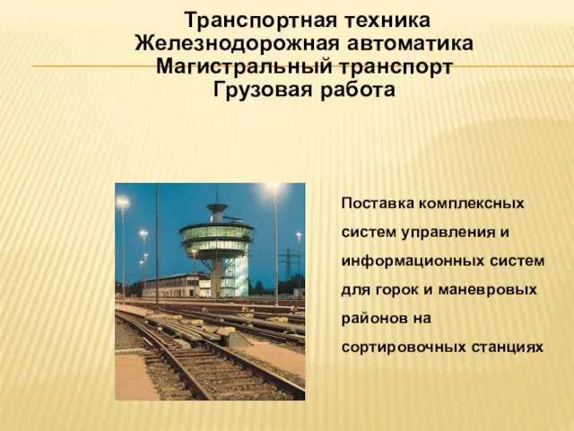 Транспортная техника. Железнодорожная автоматика. Магистральный транспорт. Грузовая работа
 Фасовочно-упаковочное оборудование торговых предприятий
 k1617989059