- Advanced x86. BIOS and System Management Mode Internals Reset Vector

Содержание
- 2. All materials are licensed under a Creative Commons “Share Alike” license. http://creativecommons.org/licenses/by-sa/3.0/ Attribution condition: You must
- 3. Reset Vector Execution Environment
- 4. Real-Address Mode (Real Mode) The original x86 operating mode Referred to as “Real Mode” for short
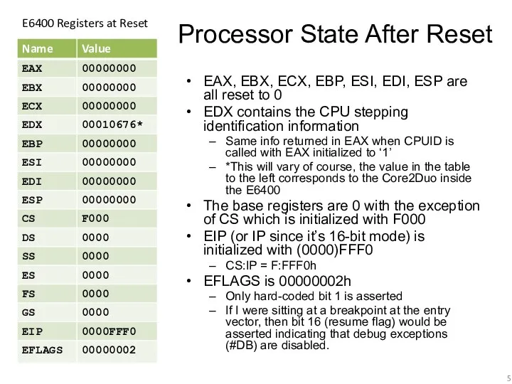
- 5. Processor State After Reset EAX, EBX, ECX, EBP, ESI, EDI, ESP are all reset to 0
- 6. Control registers CR2, CR3, and CR4 are all 0 CR0 is 6000_0010h (likely since Pentium) Paging
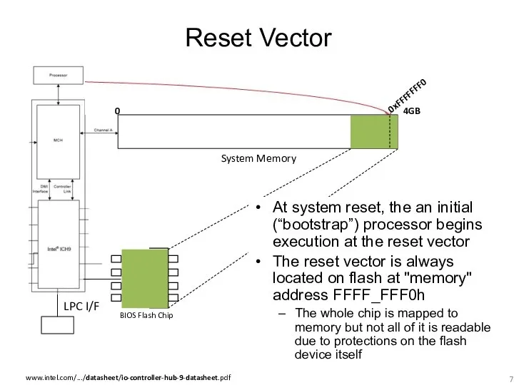
- 7. Reset Vector System Memory BIOS Flash Chip 0 4GB www.intel.com/.../datasheet/io-controller-hub-9-datasheet.pdf 0xFFFFFFF0 LPC I/F At system reset,
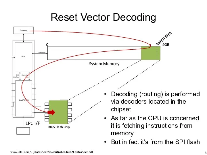
- 8. Reset Vector Decoding System Memory BIOS Flash Chip 0 4GB www.intel.com/.../datasheet/io-controller-hub-9-datasheet.pdf 0xFFFFFFF0 LPC I/F Decoding (routing)
- 9. Aside: Forensics People If the top of memory always contains a memory-mapped copy of part of
- 10. Let’s look at some of the decoding (routing) of the BIOS to memory Open RW Everything
- 11. Offset D8-D9h is FWH_DEC_EN1 As stated, this controls the decoding of ranges to the FWH If
- 12. Mini-Lab: BIOS Flash Decoding Therefore, with FWH_DEC_EN bit 14 asserted, we’re decoding to a portion of
- 13. De-assert bit 14 (set to 0xBFCC) Decoded to memory now This memory range is still read-only
- 14. Reset it back to 0xFFCC Couple of notes: Your original values may differ since BIOS flips
- 15. Mini-data-collection Lab: Reset Vector in BIOS Binary If we dump the BIOS and look at it
- 16. Real Mode Memory 16-bit operating mode Segmented memory model When operating in real-address mode, the default
- 17. Real Mode Addressing: Segment Registers CS, DS, SS, ES, FS, GS Only six segments can be
- 18. Real Mode Addressing Intel Developers Manual, 20.1.1 As shown in Figure 20-1 in the Intel SW
- 19. Real Mode Addressing Problem: Overlap Intel Developers Manual, 20.1.1 Addresses in different segments can overlap Given
- 20. F:FFF0 != FFFF:FFF0 Every segment register has a “visible” part and a “hidden” part. Intel sometimes
- 21. Descriptor Cache “When a segment selector is loaded into the visible part of a segment register,
- 22. CS.BASE + EIP CS.BASE is pre-set to FFFF_0000H upon CPU reset/power-up EIP set to 0000_FFF0H So
- 23. Reset Vector So upon startup, while the processor stays in Real Mode, it can access only
- 24. Analyzing any x86 BIOS Binary With UEFI we can usually skip straight to analyzing code we
- 25. A dream deferred We’re going to hold off on the rest of the entry vector analysis
- 26. 1: Disassemble the BIOS Binary Acquire a dump of the BIOS flash from a tool like
- 27. FIXME Update procedure for new IDA demo 6.6
- 28. 2: Rebase the Program First thing we’re going to do is rebase the program We know
- 29. 2.1: Rebase the Program In this lab our file contains only the BIOS portion of the
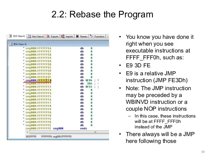
- 30. 2.2: Rebase the Program You know you have done it right when you see executable instructions
- 31. 3. Determine IDA Segments: Manually Analyze the Reset Vector JMP So now we want to create
- 32. 3.1: JMP rel16 The address following our JMP instruction is FFFF_FFF3h We’ll treat it like a
- 33. 3.2: Determine Segment Boundary So we know the destination of the JMP at the entry vector
- 34. 4: Create Initial 16-bit Segment Edit –> Segments –> Create Segment Pick any segment name you
- 35. 5: Identify Memory Model Once this segment is created, IDA “automagically” recognizes the destination of the
- 36. 5.1: LGDT Instruction LGDT loads the values in the source operand into the global descriptor table
- 37. 5.2: Import GDT/IDT Structures You can import these structures into IDA by parsing the file “descriptors.h”
- 38. 5.3: Define GdtPtr Go to the address referenced by the operand to the LGDT instruction IDA
- 39. 5.4: Define GDT Entries We know it’s location is in our 16-bit segment Manually go there
- 40. 5.5: Full GDT The GdtEntry structure definition in peewee.h can be used to interpret the GDT
- 41. 5.5: Full GDT Here is the entire GDT for reference. You don’t need an expensive debugger
- 42. 6: Create the 32-bit BIOS segment Now create the 32-bit segment Start address is FFFF_FFFFh -
- 43. 7: Touch up the Far Jump So we know that this is loading the descriptor entry
- 44. Welcome to BIOS Analysis Converting the binary at FFFF_0100h to code provides you the entry point
- 45. Why so Ugly? IDA Segments IDA can’t combine 16-bit and 32-bit instructions in the same segment
- 46. BIOS Reset Vector Analysis: Short Cut 1 You can likely skip a few of the steps
- 47. BIOS Reset Vector Analysis: Short Cut 2 Follow the entry JMP Notice that IDA automagically modified
- 49. Скачать презентацию
All materials are licensed under a Creative Commons “Share Alike” license.
http://creativecommons.org/licenses/by-sa/3.0/
Attribution
All materials are licensed under a Creative Commons “Share Alike” license.
http://creativecommons.org/licenses/by-sa/3.0/
Attribution
Reset Vector
Execution Environment
Reset Vector
Execution Environment
Real-Address Mode (Real Mode)
The original x86 operating mode
Referred to as “Real
Real-Address Mode (Real Mode)
The original x86 operating mode
Referred to as “Real
Processor State After Reset
EAX, EBX, ECX, EBP, ESI, EDI, ESP are
Processor State After Reset
EAX, EBX, ECX, EBP, ESI, EDI, ESP are
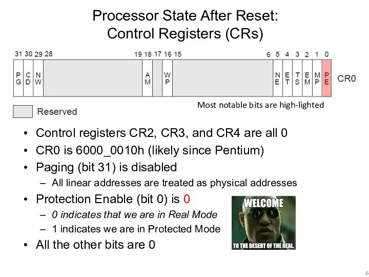
Control registers CR2, CR3, and CR4 are all 0
CR0 is
Control registers CR2, CR3, and CR4 are all 0
CR0 is
Reset Vector
System Memory
BIOS Flash Chip
0
4GB
www.intel.com/.../datasheet/io-controller-hub-9-datasheet.pdf
0xFFFFFFF0
LPC I/F
At system reset, the an initial
Reset Vector
System Memory
BIOS Flash Chip
0
4GB
www.intel.com/.../datasheet/io-controller-hub-9-datasheet.pdf
0xFFFFFFF0
LPC I/F
At system reset, the an initial
Reset Vector Decoding
System Memory
BIOS Flash Chip
0
4GB
www.intel.com/.../datasheet/io-controller-hub-9-datasheet.pdf
0xFFFFFFF0
LPC I/F
Decoding (routing) is performed via
Reset Vector Decoding
System Memory
BIOS Flash Chip
0
4GB
www.intel.com/.../datasheet/io-controller-hub-9-datasheet.pdf
0xFFFFFFF0
LPC I/F
Decoding (routing) is performed via
Aside: Forensics People
If the top of memory always contains a memory-mapped
Aside: Forensics People
If the top of memory always contains a memory-mapped
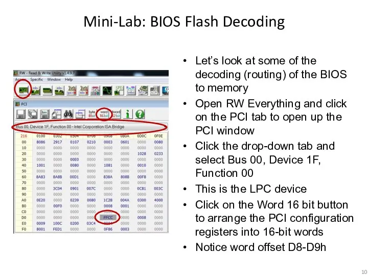
Let’s look at some of the decoding (routing) of the BIOS
Let’s look at some of the decoding (routing) of the BIOS
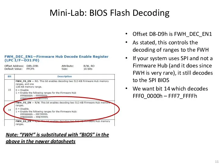
Offset D8-D9h is FWH_DEC_EN1
As stated, this controls the decoding of ranges
Offset D8-D9h is FWH_DEC_EN1
As stated, this controls the decoding of ranges
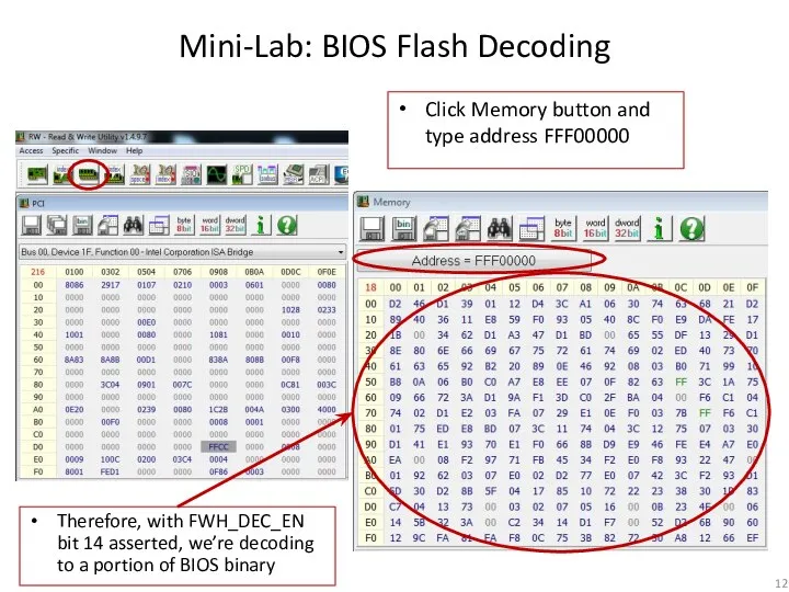
Mini-Lab: BIOS Flash Decoding
Therefore, with FWH_DEC_EN bit 14 asserted, we’re decoding
Mini-Lab: BIOS Flash Decoding
Therefore, with FWH_DEC_EN bit 14 asserted, we’re decoding
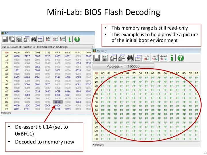
De-assert bit 14 (set to 0xBFCC)
Decoded to memory now
This memory range
De-assert bit 14 (set to 0xBFCC)
Decoded to memory now
This memory range
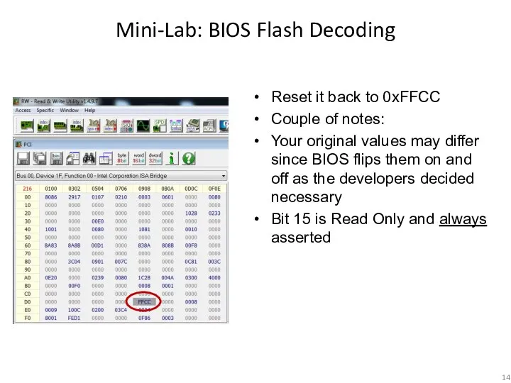
Reset it back to 0xFFCC
Couple of notes:
Your original values may differ
Reset it back to 0xFFCC
Couple of notes:
Your original values may differ
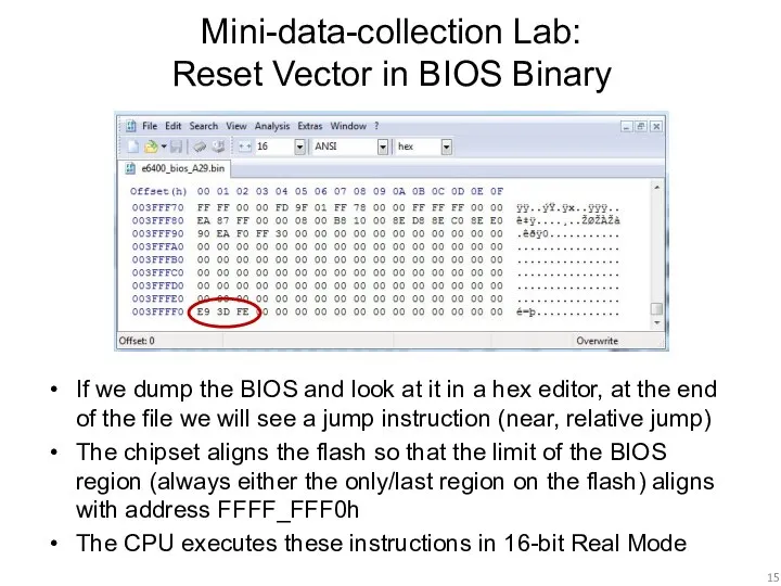
Mini-data-collection Lab:
Reset Vector in BIOS Binary
If we dump the BIOS and
Mini-data-collection Lab:
Reset Vector in BIOS Binary
If we dump the BIOS and
Real Mode Memory
16-bit operating mode
Segmented memory model
When operating in real-address mode,
Real Mode Memory
16-bit operating mode
Segmented memory model
When operating in real-address mode,
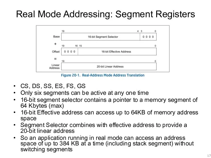
Real Mode Addressing: Segment Registers
CS, DS, SS, ES, FS, GS
Only six
Real Mode Addressing: Segment Registers
CS, DS, SS, ES, FS, GS
Only six
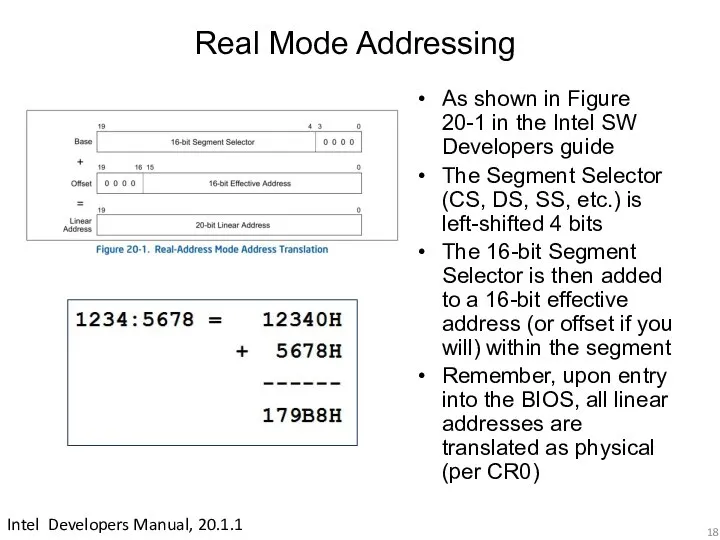
Real Mode Addressing
Intel Developers Manual, 20.1.1
As shown in Figure 20-1 in
Real Mode Addressing
Intel Developers Manual, 20.1.1
As shown in Figure 20-1 in
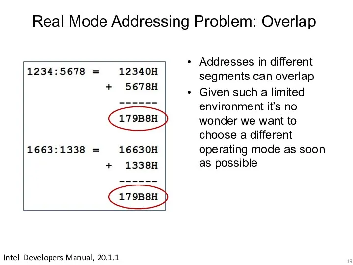
Real Mode Addressing Problem: Overlap
Intel Developers Manual, 20.1.1
Addresses in different segments
Real Mode Addressing Problem: Overlap
Intel Developers Manual, 20.1.1
Addresses in different segments
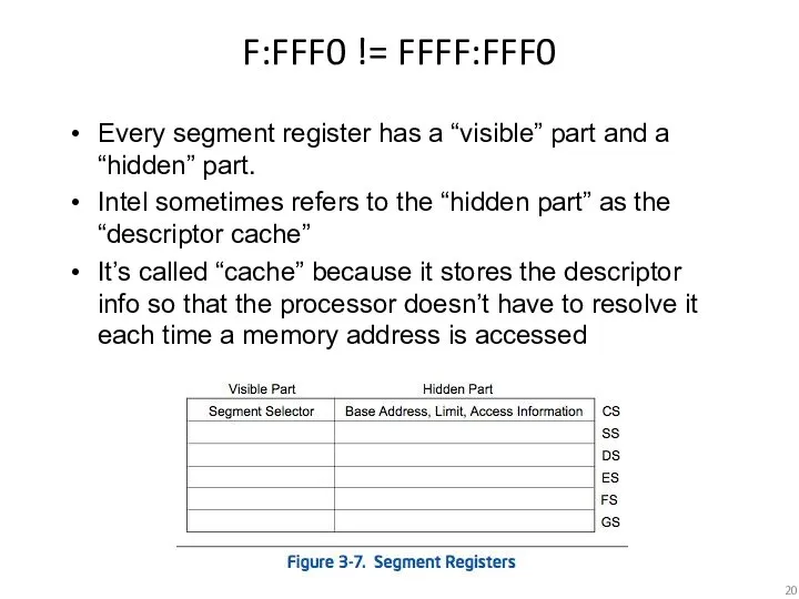
F:FFF0 != FFFF:FFF0
Every segment register has a “visible” part and a
F:FFF0 != FFFF:FFF0
Every segment register has a “visible” part and a
Descriptor Cache
“When a segment selector is loaded into the visible part
Descriptor Cache
“When a segment selector is loaded into the visible part
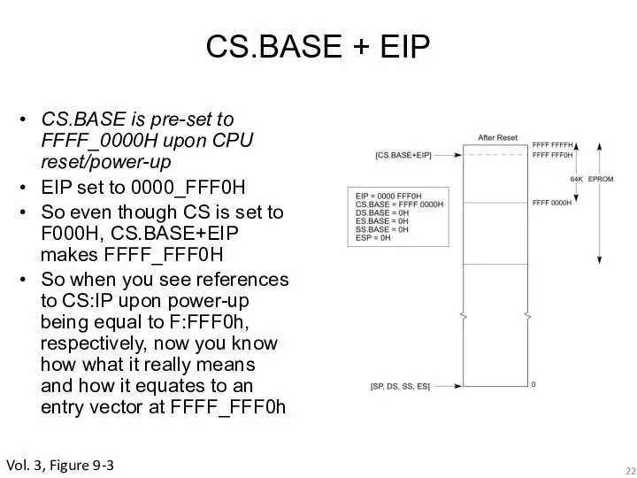
CS.BASE + EIP
CS.BASE is pre-set to FFFF_0000H upon CPU reset/power-up
EIP set
CS.BASE + EIP
CS.BASE is pre-set to FFFF_0000H upon CPU reset/power-up
EIP set
Reset Vector
So upon startup, while the processor stays in Real Mode,
Reset Vector
So upon startup, while the processor stays in Real Mode,
Analyzing any x86 BIOS Binary
With UEFI we can usually skip straight
Analyzing any x86 BIOS Binary
With UEFI we can usually skip straight
A dream deferred
We’re going to hold off on the rest of
A dream deferred
We’re going to hold off on the rest of
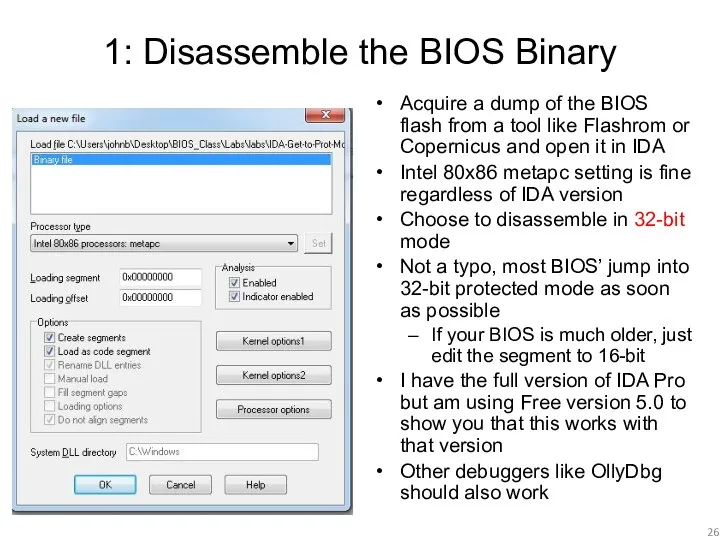
1: Disassemble the BIOS Binary
Acquire a dump of the BIOS flash
1: Disassemble the BIOS Binary
Acquire a dump of the BIOS flash
FIXME
Update procedure for new IDA demo 6.6
FIXME
Update procedure for new IDA demo 6.6
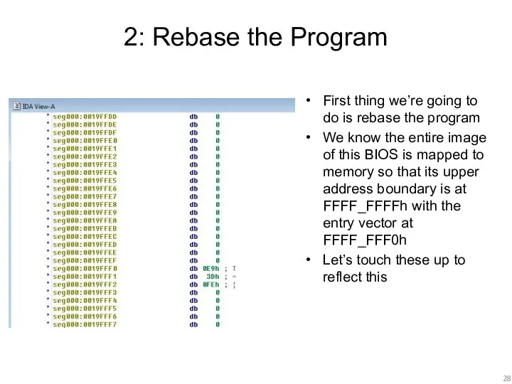
2: Rebase the Program
First thing we’re going to do is rebase
2: Rebase the Program
First thing we’re going to do is rebase
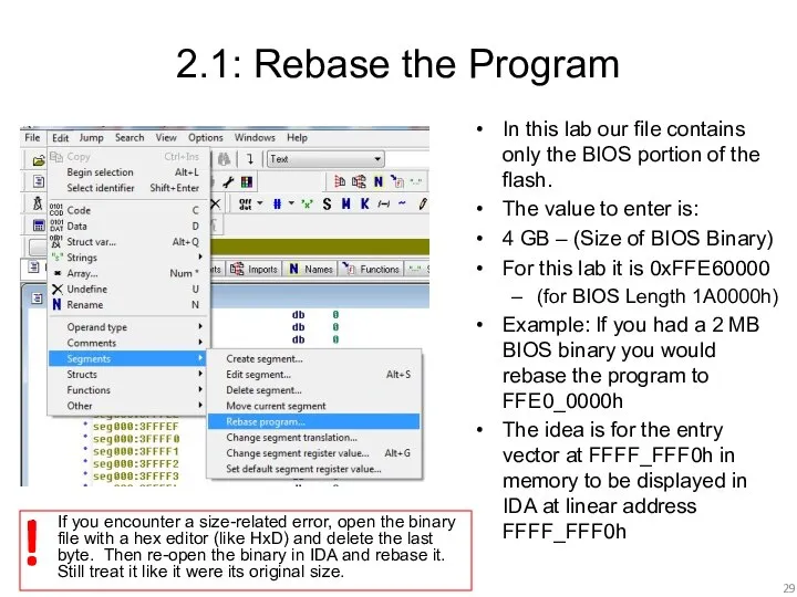
2.1: Rebase the Program
In this lab our file contains only the
2.1: Rebase the Program
In this lab our file contains only the
2.2: Rebase the Program
You know you have done it right when
2.2: Rebase the Program
You know you have done it right when
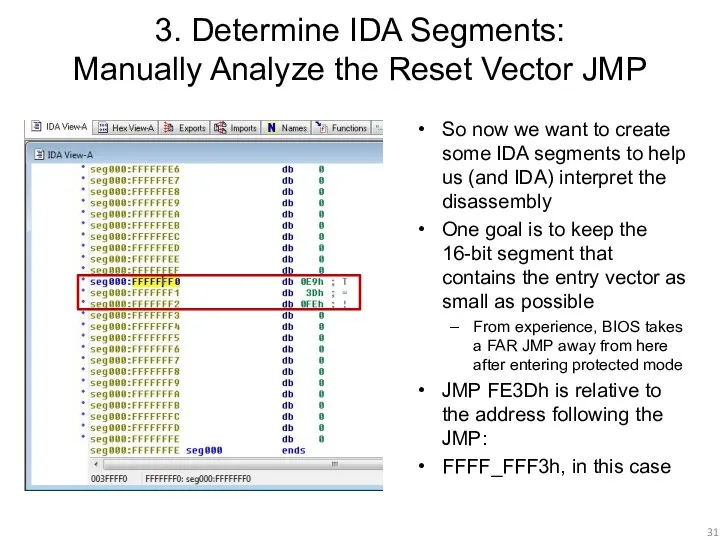
3. Determine IDA Segments:
Manually Analyze the Reset Vector JMP
So now
3. Determine IDA Segments:
Manually Analyze the Reset Vector JMP
So now
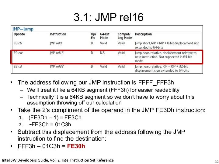
3.1: JMP rel16
The address following our JMP instruction is FFFF_FFF3h
We’ll
3.1: JMP rel16
The address following our JMP instruction is FFFF_FFF3h
We’ll
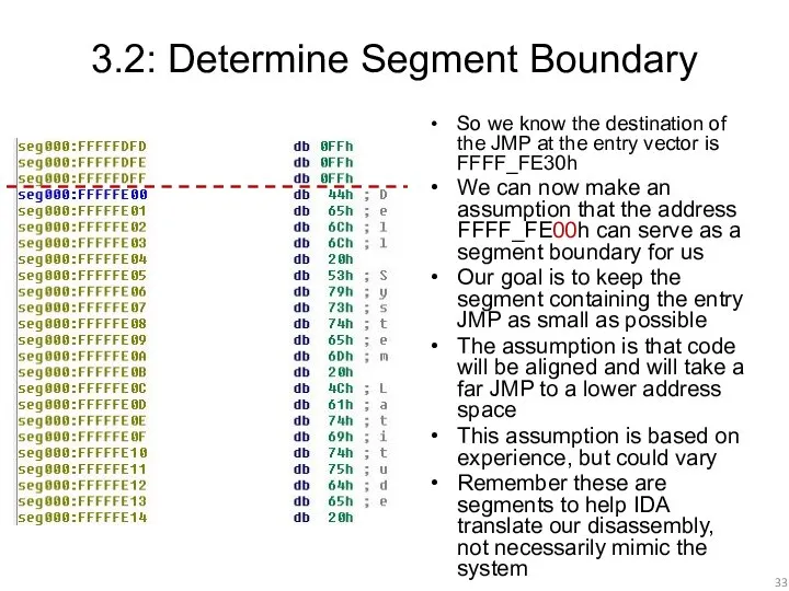
3.2: Determine Segment Boundary
So we know the destination of the JMP
3.2: Determine Segment Boundary
So we know the destination of the JMP
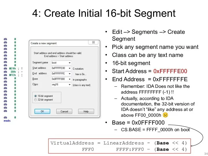
4: Create Initial 16-bit Segment
Edit –> Segments –> Create Segment
Pick any
4: Create Initial 16-bit Segment
Edit –> Segments –> Create Segment
Pick any
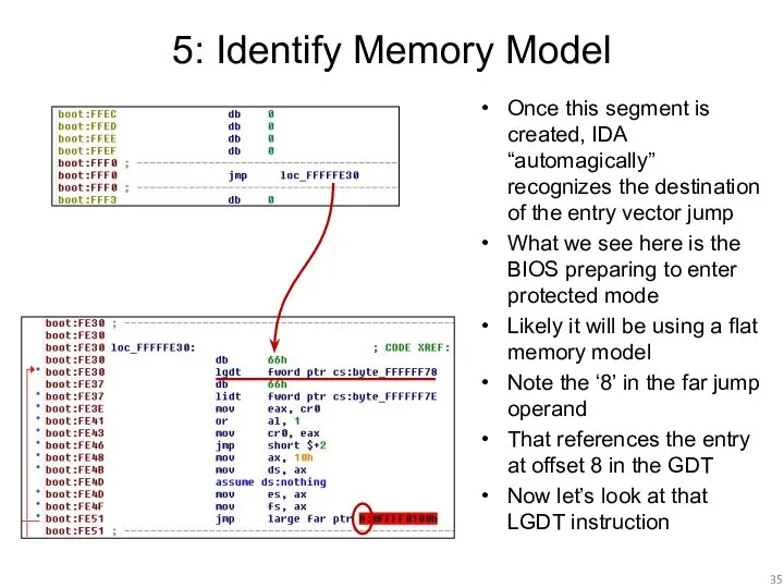
5: Identify Memory Model
Once this segment is created, IDA “automagically” recognizes
5: Identify Memory Model
Once this segment is created, IDA “automagically” recognizes
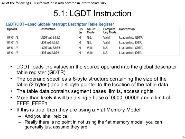
5.1: LGDT Instruction
LGDT loads the values in the source operand into
5.1: LGDT Instruction
LGDT loads the values in the source operand into
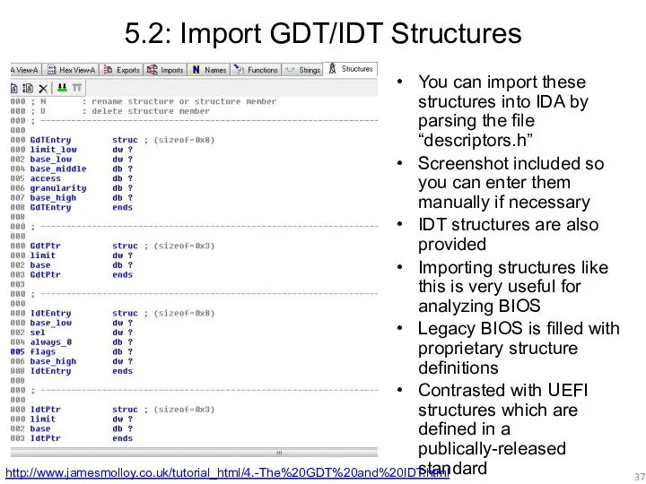
5.2: Import GDT/IDT Structures
You can import these structures into IDA by
5.2: Import GDT/IDT Structures
You can import these structures into IDA by
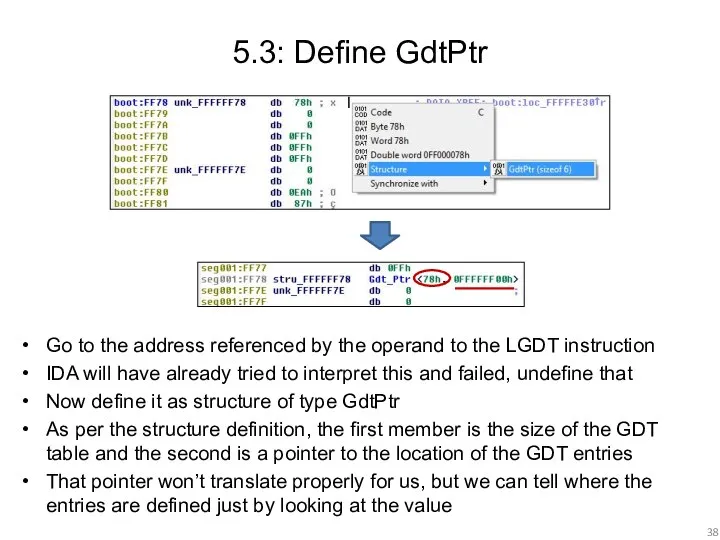
5.3: Define GdtPtr
Go to the address referenced by the operand to
5.3: Define GdtPtr
Go to the address referenced by the operand to
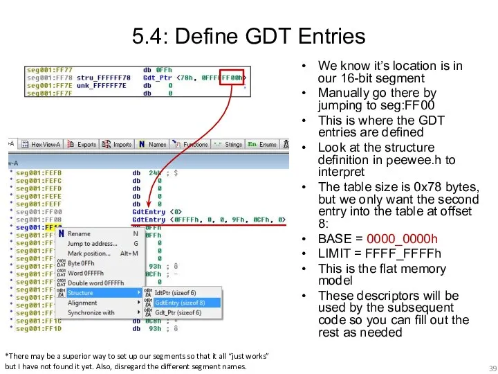
5.4: Define GDT Entries
We know it’s location is in our 16-bit
5.4: Define GDT Entries
We know it’s location is in our 16-bit
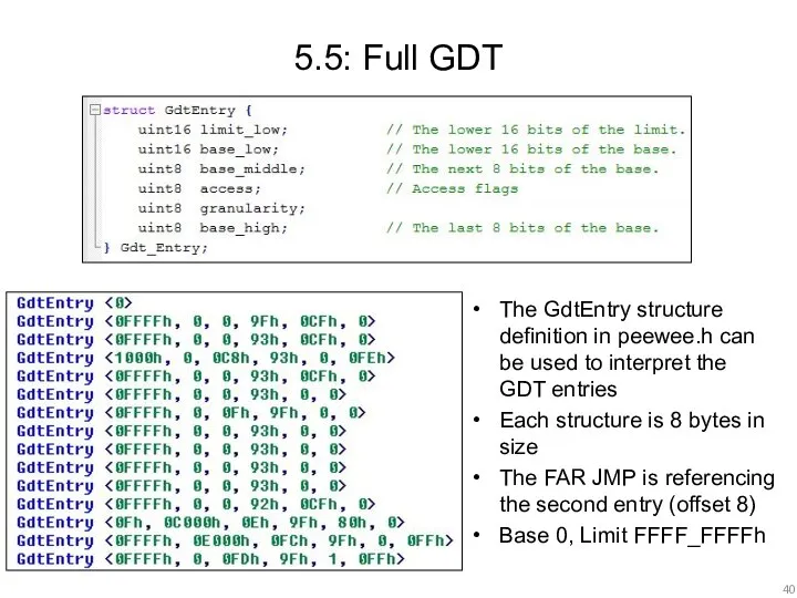
5.5: Full GDT
The GdtEntry structure definition in peewee.h can be used
5.5: Full GDT
The GdtEntry structure definition in peewee.h can be used
5.5: Full GDT
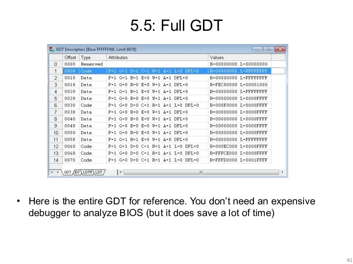
Here is the entire GDT for reference. You don’t
5.5: Full GDT
Here is the entire GDT for reference. You don’t
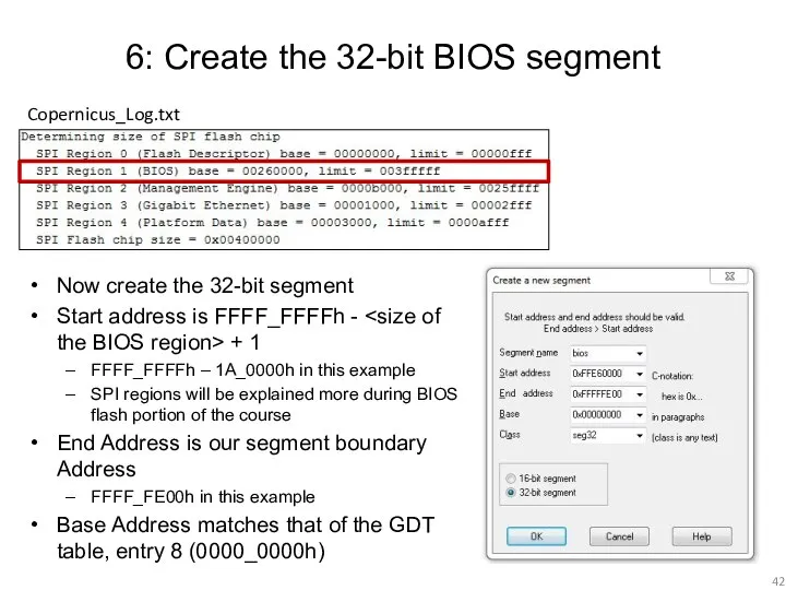
6: Create the 32-bit BIOS segment
Now create the 32-bit segment
Start address
6: Create the 32-bit BIOS segment
Now create the 32-bit segment
Start address
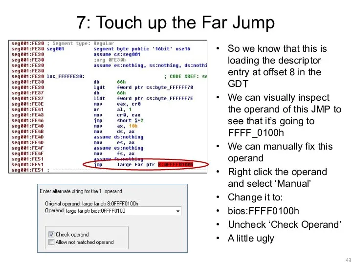
7: Touch up the Far Jump
So we know that this is
7: Touch up the Far Jump
So we know that this is
Welcome to BIOS Analysis
Converting the binary at FFFF_0100h to code provides
Welcome to BIOS Analysis
Converting the binary at FFFF_0100h to code provides
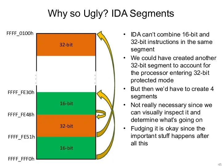
Why so Ugly? IDA Segments
IDA can’t combine 16-bit and 32-bit instructions
Why so Ugly? IDA Segments
IDA can’t combine 16-bit and 32-bit instructions
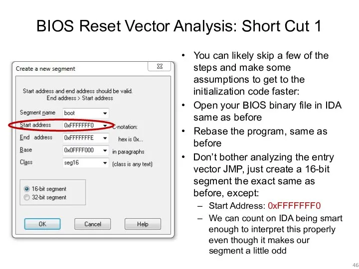
BIOS Reset Vector Analysis: Short Cut 1
You can likely skip a
BIOS Reset Vector Analysis: Short Cut 1
You can likely skip a
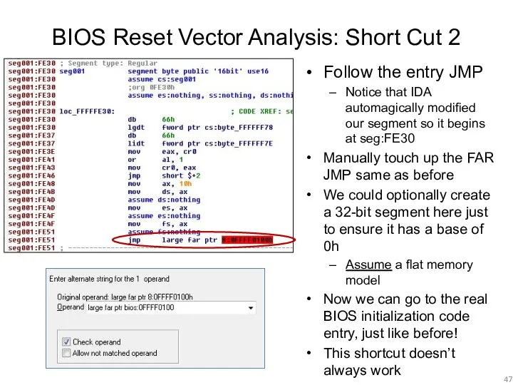
BIOS Reset Vector Analysis: Short Cut 2
Follow the entry JMP
Notice that
BIOS Reset Vector Analysis: Short Cut 2
Follow the entry JMP
Notice that
 СМС НА ЕКРАНАХ ЗАЛУЧЕННЯ АУДИТОРІЇ ДО ІНТЕРАКТИВНОГО СПІЛКУВАННЯ
 Система нормативных документов в строительстве. (Лекция 7)
 Прикладное значение занятий физической культурой для профилактики и лечения сколиоза
 Изобразительное искусство древнего Рима
 Презентация по алгебре Квадратичная функция
  Spisok_Artistov
 ГТО – путь к успеху
 Глоссарий. Предпринимательские термины на тему: Визуализация мышления и информационный дизайн
 Конструктивные схемы гелиевых криостатов
 Общие сведения о производстве сборных железобетонных изделий
 Поршневая группа
 C Послеродовой уход
 Золотое сечение в архитектуре
 Приключения Бертольдо - презентация для начальной школы
 Культурно-историческое наследие Удомельского района. Алексей Гаврилович Венецианов
 Можно ли учить «по-всякому»
 Праця підлітків
 Презентация "Покупательское поведение на рынках" - скачать презентации по Экономике
 Токовые защиты. Принцип действия и классификация токовых защит
 Феликс Баумгартнер
 Страхование грузов
 Футбол. Без футбола жить нельзя
 Презентация Духовная жизнь общества
 Путешествие по Транссибирской железной дороге из Москвы во Владивосток
 Михаил Васильевич Ломоносов (1711-1765). Викторина по математике
 Презентация по теме Mein Zuhause по немецкому языку в 6 классе
 Презентация на тему "Программа учебной дисциплины (название дисциплины)" - скачать презентации по Педагогике
 Методы программирования. Алгоритмы поиска. (Лекция 5)