- Evolution of implementation technologies

Содержание
- 2. Xilinx FPGAs - Gate Array Technology (IBM - 1970s) Simple logic gates combine transistors to implement
- 3. Xilinx FPGAs - Field-Programmable Gate Arrays Logic blocks to implement combinational and sequential logic Interconnect wires
- 4. Xilinx FPGAs - Enabling Technology Cheap/fast fuse connections small area (can fit lots of them) low
- 5. Xilinx FPGAs - Programming Technologies Fuse and anti-fuse fuse makes or breaks link between two wires
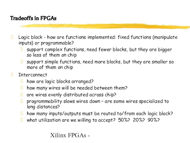
- 6. Xilinx FPGAs - Tradeoffs in FPGAs Logic block - how are functions implemented: fixed functions (manipulate
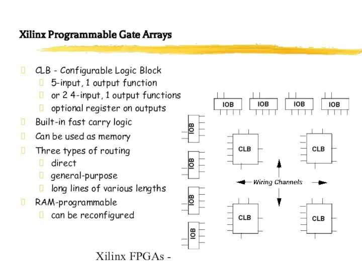
- 7. Xilinx FPGAs - Xilinx Programmable Gate Arrays CLB - Configurable Logic Block 5-input, 1 output function
- 8. Xilinx FPGAs -
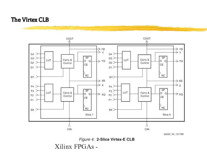
- 9. Xilinx FPGAs - The Virtex CLB
- 10. Xilinx FPGAs - Details of One Virtex Slice
- 11. Xilinx FPGAs - Implements any Two 4-input Functions 4-input function 3-input function; registered
- 12. Xilinx FPGAs - Implements any 5-input Function 5-input function
- 13. Xilinx FPGAs - Implement Some Larger Functions e.g. 9-input parity
- 14. Xilinx FPGAs - Two Slices: Any 6-input Function 6-input function from other slice
- 15. Xilinx FPGAs - Two Slices: Implement some larger functions e.g. 19-input parity from other slice
- 16. Xilinx FPGAs - Fast Carry Chain: Add two bits per slice Sum(a,b,cin) Carry(a,b,cin) a b cin
- 17. Xilinx FPGAs - Lookup Tables used as memory (16 x 2) [ Distributed Memory ]
- 18. Xilinx FPGAs - Lookup Tables used as memory (32 x 1)
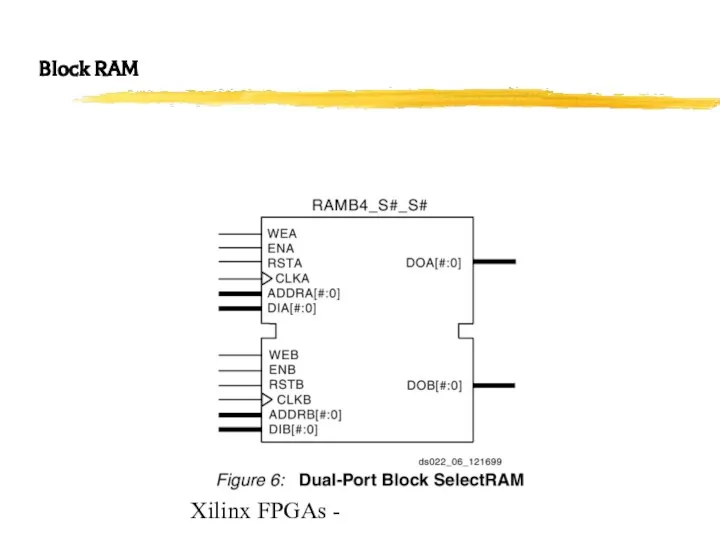
- 19. Xilinx FPGAs - Block RAM
- 20. Xilinx FPGAs - Virtex Routing
- 21. Xilinx FPGAs - Virtex Routing
- 22. Xilinx FPGAs - Non-Local Routing Hex wires Extend 6 CLBs in one direction Connections at 3
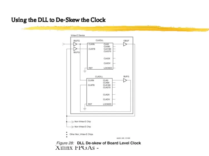
- 23. Xilinx FPGAs - Using the DLL to De-Skew the Clock
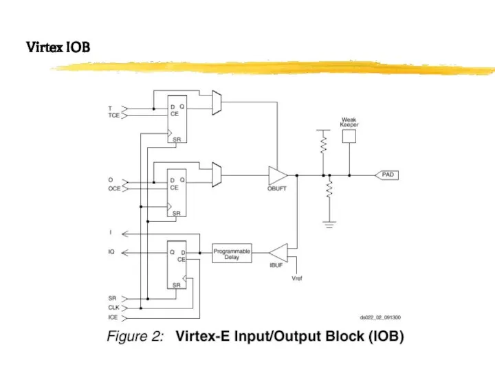
- 24. Xilinx FPGAs - Virtex IOB
- 25. Xilinx FPGAs - Computer-aided Design Can't design FPGAs by hand way too much logic to manage,
- 26. Xilinx FPGAs - CAD Tool Path (cont’d) Placement and routing assign logic blocks to functions make
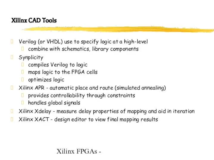
- 27. Xilinx FPGAs - Xilinx CAD Tools Verilog (or VHDL) use to specify logic at a high-level
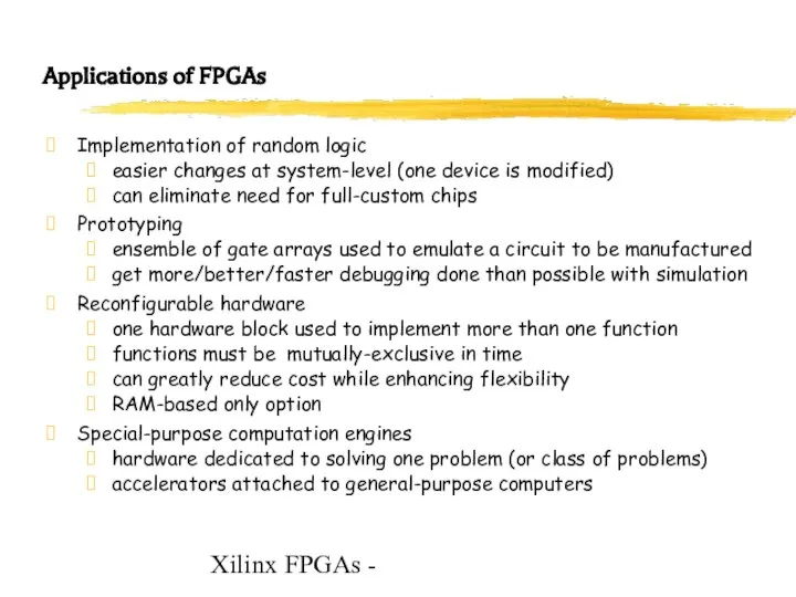
- 28. Xilinx FPGAs - Applications of FPGAs Implementation of random logic easier changes at system-level (one device
- 30. Скачать презентацию
Xilinx FPGAs -
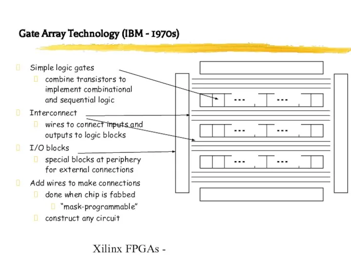
Gate Array Technology (IBM - 1970s)
Simple logic gates
combine
Xilinx FPGAs -
Gate Array Technology (IBM - 1970s)
Simple logic gates
combine
Xilinx FPGAs -
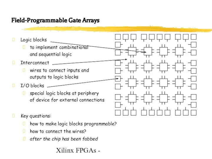
Field-Programmable Gate Arrays
Logic blocks
to implement combinational
and sequential logic
Interconnect
wires
Xilinx FPGAs -
Field-Programmable Gate Arrays
Logic blocks
to implement combinational
and sequential logic
Interconnect
wires
Xilinx FPGAs -
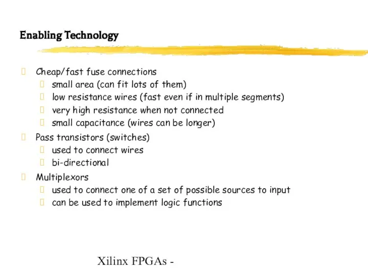
Enabling Technology
Cheap/fast fuse connections
small area (can fit lots
Xilinx FPGAs -
Enabling Technology
Cheap/fast fuse connections
small area (can fit lots
Xilinx FPGAs -
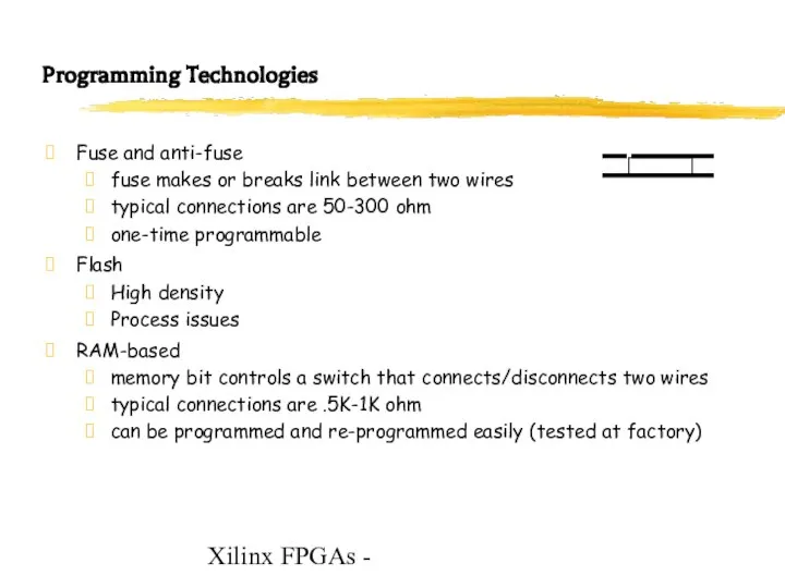
Programming Technologies
Fuse and anti-fuse
fuse makes or breaks link
Xilinx FPGAs -
Programming Technologies
Fuse and anti-fuse
fuse makes or breaks link
Xilinx FPGAs -
Tradeoffs in FPGAs
Logic block - how are functions
Xilinx FPGAs -
Tradeoffs in FPGAs
Logic block - how are functions
Xilinx FPGAs -
Xilinx Programmable Gate Arrays
CLB - Configurable Logic Block
5-input,
Xilinx FPGAs -
Xilinx Programmable Gate Arrays
CLB - Configurable Logic Block
5-input,
Xilinx FPGAs -
Xilinx FPGAs -
Xilinx FPGAs -
The Virtex CLB
Xilinx FPGAs -
The Virtex CLB
Xilinx FPGAs -
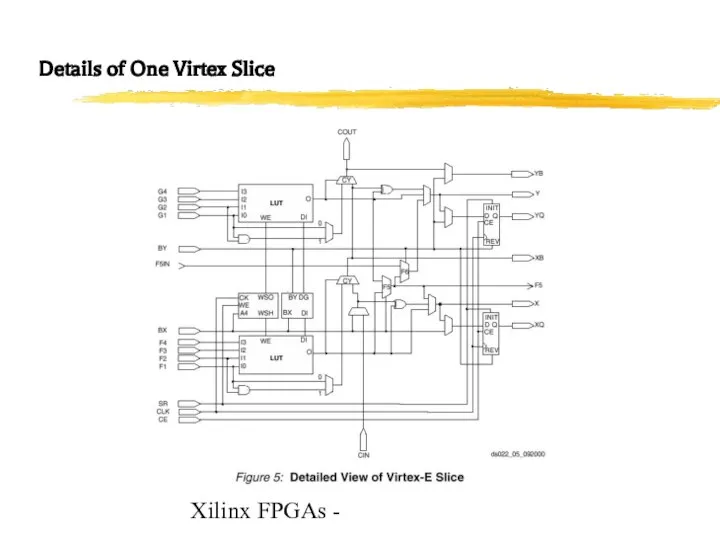
Details of One Virtex Slice
Xilinx FPGAs -
Details of One Virtex Slice
Xilinx FPGAs -
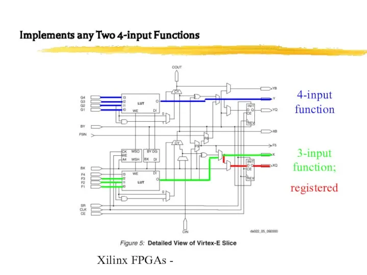
Implements any Two 4-input Functions
4-input function
3-input function;
registered
Xilinx FPGAs -
Implements any Two 4-input Functions
4-input function
3-input function;
registered
Xilinx FPGAs -
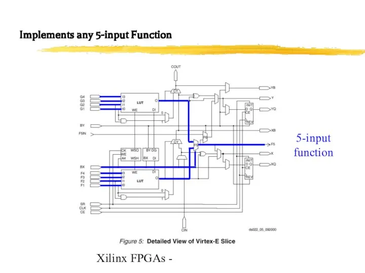
Implements any 5-input Function
5-input function
Xilinx FPGAs -
Implements any 5-input Function
5-input function
Xilinx FPGAs -
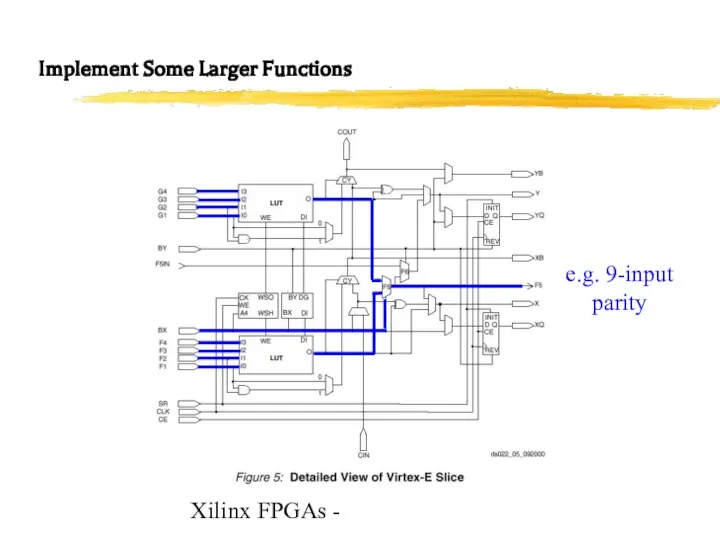
Implement Some Larger Functions
e.g. 9-input parity
Xilinx FPGAs -
Implement Some Larger Functions
e.g. 9-input parity
Xilinx FPGAs -
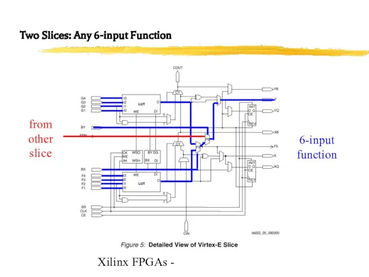
Two Slices: Any 6-input Function
6-input function
from other slice
Xilinx FPGAs -
Two Slices: Any 6-input Function
6-input function
from other slice
Xilinx FPGAs -
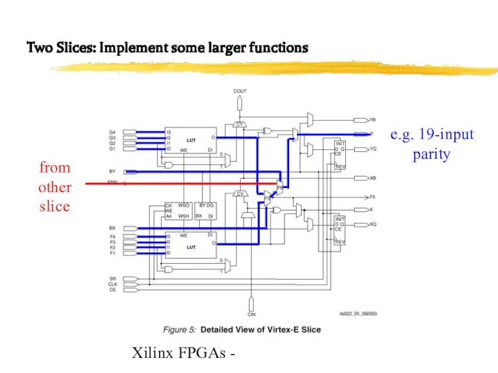
Two Slices: Implement some larger functions
e.g. 19-input parity
from
Xilinx FPGAs -
Two Slices: Implement some larger functions
e.g. 19-input parity
from
Xilinx FPGAs -
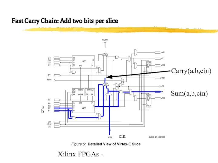
Fast Carry Chain: Add two bits per slice
Sum(a,b,cin)
Carry(a,b,cin)
a
b
cin
Xilinx FPGAs -
Fast Carry Chain: Add two bits per slice
Sum(a,b,cin)
Carry(a,b,cin)
a
b
cin
![Xilinx FPGAs - Lookup Tables used as memory (16 x 2) [ Distributed Memory ]](/_ipx/f_webp&q_80&fit_contain&s_1440x1080/imagesDir/jpg/1365318/slide-16.jpg)
Xilinx FPGAs -
Lookup Tables used as memory (16 x 2)
[
Xilinx FPGAs -
Lookup Tables used as memory (16 x 2) [
Xilinx FPGAs -
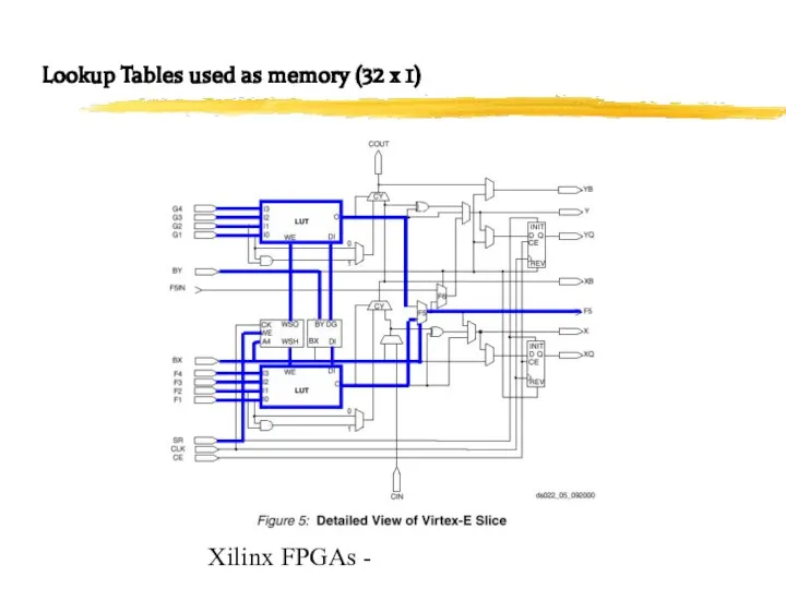
Lookup Tables used as memory (32 x 1)
Xilinx FPGAs -
Lookup Tables used as memory (32 x 1)
Xilinx FPGAs -
Block RAM
Xilinx FPGAs -
Block RAM
Xilinx FPGAs -
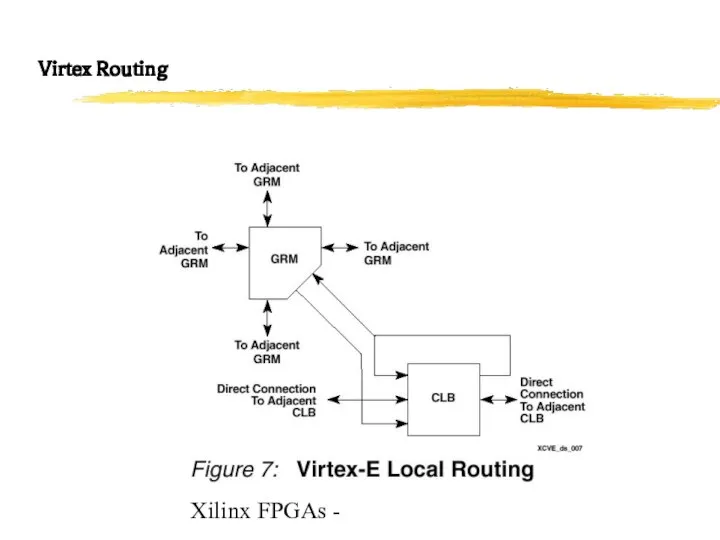
Virtex Routing
Xilinx FPGAs -
Virtex Routing
Xilinx FPGAs -
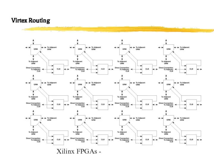
Virtex Routing
Xilinx FPGAs -
Virtex Routing
Xilinx FPGAs -
Non-Local Routing
Hex wires
Extend 6 CLBs in one direction
Connections
Xilinx FPGAs -
Non-Local Routing
Hex wires
Extend 6 CLBs in one direction
Connections
Xilinx FPGAs -
Using the DLL to De-Skew the Clock
Xilinx FPGAs -
Using the DLL to De-Skew the Clock
Xilinx FPGAs -
Virtex IOB
Xilinx FPGAs -
Virtex IOB
Xilinx FPGAs -
Computer-aided Design
Can't design FPGAs by hand
way too much
Xilinx FPGAs -
Computer-aided Design
Can't design FPGAs by hand
way too much
Xilinx FPGAs -
CAD Tool Path (cont’d)
Placement and routing
assign logic blocks
Xilinx FPGAs -
CAD Tool Path (cont’d)
Placement and routing
assign logic blocks
Xilinx FPGAs -
Xilinx CAD Tools
Verilog (or VHDL) use to specify
Xilinx FPGAs -
Xilinx CAD Tools
Verilog (or VHDL) use to specify
Xilinx FPGAs -
Applications of FPGAs
Implementation of random logic
easier changes at
Xilinx FPGAs -
Applications of FPGAs
Implementation of random logic
easier changes at
 Связь явлений Часть 1
 Материнская плата
 Презентация "Карманные деньги" - скачать презентации по Экономике
 КРОССВОРД Голофаст Н. и Зорина Д.
  Політичний портрет Віктора Ющенка
 Реализация алгоритма блочного шифрования на основе сплайн-вейвлетов в ОС Windows
  Семейства ЭВМ
 Земляные работы
 Методы обследования памяти
  Специфика гетерономной этики
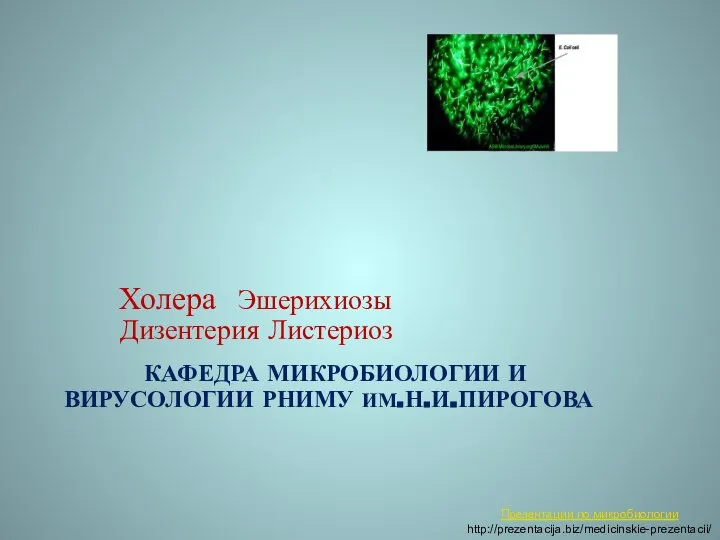 кафедра микробиологии и вирусологии РНИМУ им.Н.И.Пирогова Холера Эшерихиозы Дизентерия Листериоз
  Общая характеристика Римской курии
 Презентация Классицизм
 Политические деятели США
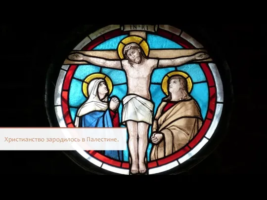 Первые века христианства
 Преступления против общественной безопасности (ст. 205-227 УК РФ
 Цыпленок и утенок - презентация для начальной школы
 Святитель Лука Войно-Ясенецкий 1877 - 1961
 История как наука
 шахматная нотация
 Презентация "Анализ и диагностика финансово-хозяйственной деятельности предприятия. Методика определения величины хозяйствен
 Приволжский федеральный округ Выполнили: студент ФТД-4 группы Т-093 Воробьев Д.Н., Карташова Г.С., Ивантей М.И.
  Функции, события. Тема 1.6
 Rok liturgiczny
 Священные сооружения: буддийский храм
 Коммуникации в организации
  Вводные предложения - презентация для начальной школы
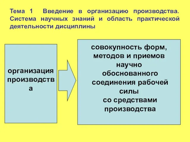 Презентация "Введение в организацию производства. Система научных знаний и область практической деятельности дисциплины" - с