- Using systemvue’s open FPGA design flow, M8190A Sig Gen, M9703A High Speed Digitizer

Содержание
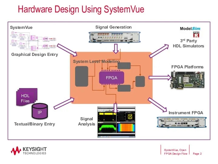
- 2. Hardware Design Using SystemVue SystemVue, Open FPGA Design Flow HDL Files IP Graphical Design Entry Textual/Binary
- 3. SystemVue Hardware Design Kit Model based graphical design tool Predict hardware behaviors, before committing to a
- 4. PART I: SystemVue Open FPGA Design Flow SystemVue, Open FPGA Design Flow
- 5. Automatic HDL Code Generation Provides path to rapid prototyping and hardware implementation Generating hierarchical VHDL/Verilog allows
- 6. SystemVue FPGA Design Flow SYSTEM LEVEL SystemVue, Open FPGA Design Flow
- 7. Various fixed point blocks for hardware design symbol mapping 1st half band filtering CIC filter CORDIC
- 8. Design Optimization Fixed Point Analysis Sweep Analysis Recursive Graphical Design Design1 Design1 Design1 Design1 Design1 SystemVue,
- 9. Demo One SystemVue general FPGA design flow Native simulation HDL co-simulation HIL co-simulation Hardware in loop
- 10. PART II: Integrated Design Flow for M9703A Digitizer SystemVue, Open FPGA Design Flow
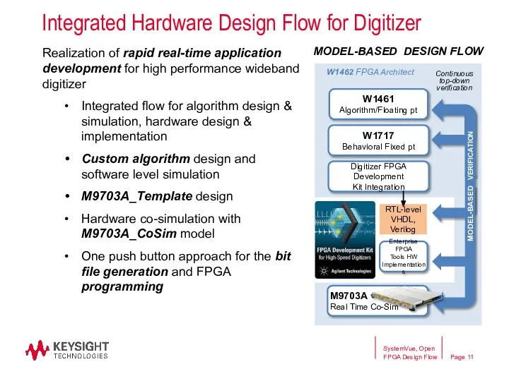
- 11. Integrated Hardware Design Flow for Digitizer Realization of rapid real-time application development for high performance wideband
- 12. Key Benefits of the integrated design flow Early development of Firmware/Software APIs before HW arrives Standard
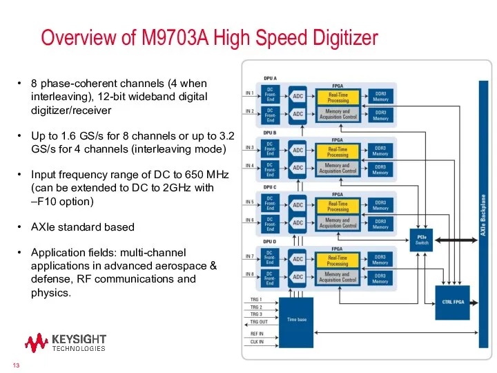
- 13. Overview of M9703A High Speed Digitizer SystemVue/FPGA Flow 8 phase-coherent channels (4 when interleaving), 12-bit wideband
- 14. DPU FPGA user core ADC input format 1-Ch mode (3.2GS/s) 2-Ch mode (1.6GS/s)
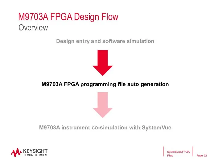
- 15. M9703A FPGA Design Flow Design entry and software simulation M9703A FPGA programming file auto generation M9703A
- 16. M9703A FPGA Design Flow Design entry and software simulation M9703A FPGA programming file auto generation M9703A
- 17. M9703A FPGA Design Flow C++ simulation or C++/HDL mixed simulation if HDL codes or Xilinx IP
- 18. M9703A FPGA Design Flow SystemVue/FPGA Flow Design entry and software simulation
- 19. M9703A FPGA Design Flow SystemVue/FPGA Flow Design entry and software simulation
- 20. M9703A FPGA Design Flow SystemVue/FPGA Flow Design entry and software simulation
- 21. M9703A FPGA Design Flow Design entry and software simulation M9703A FPGA programming file auto generation M9703A
- 22. M9703A FPGA Design Flow Design entry and software simulation M9703A FPGA programming file auto generation M9703A
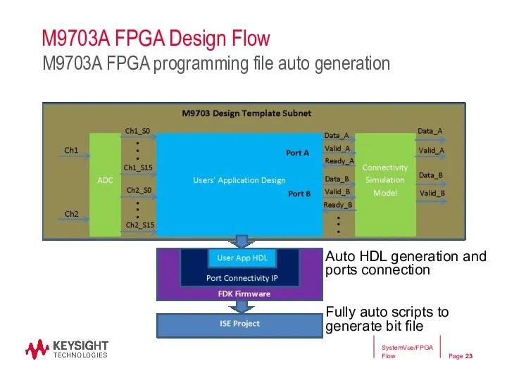
- 23. M9703A FPGA Design Flow M9703A FPGA programming file auto generation SystemVue/FPGA Flow Auto HDL generation and
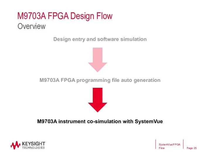
- 24. M9703A FPGA Design Flow Design entry and software simulation M9703A FPGA programming file auto generation M9703A
- 25. M9703A FPGA Design Flow Design entry and software simulation M9703A FPGA programming file auto generation M9703A
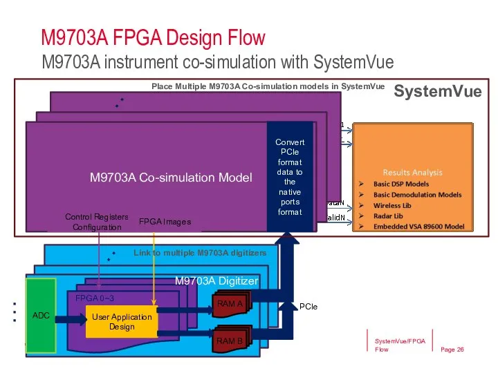
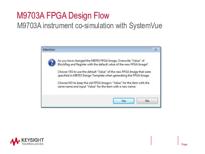
- 26. M9703A FPGA Design Flow SystemVue/FPGA Flow M9703A instrument co-simulation with SystemVue M9703 Cosim Model M9703 Cosim
- 27. M9703A FPGA Design Flow M9703A instrument co-simulation with SystemVue
- 28. M9703A FPGA Design Flow M9703A instrument co-simulation with SystemVue
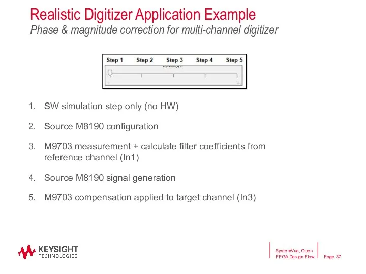
- 29. Realistic Digitizer Application Example Phase & magnitude correction for multi-channel digitizer AD DDC FIR W Φ
- 30. Realistic Digitizer Application Example Phase & magnitude correction for multi-channel digitizer What is difference between channels?
- 31. Realistic Digitizer Application Example Phase & magnitude correction for multi-channel digitizer Signal processing Trigger Sequence ……
- 32. Realistic Digitizer Application Example Phase & magnitude correction for multi-channel digitizer Block diagram Halfband FIR1 1.6GSaPS
- 33. SystemVue, Open FPGA Design Flow Realistic Digitizer Application Example Phase & magnitude correction for multi-channel digitizer
- 34. SystemVue, Open FPGA Design Flow Required Hardware: M9703 with FDK option to enable its FPGA programming
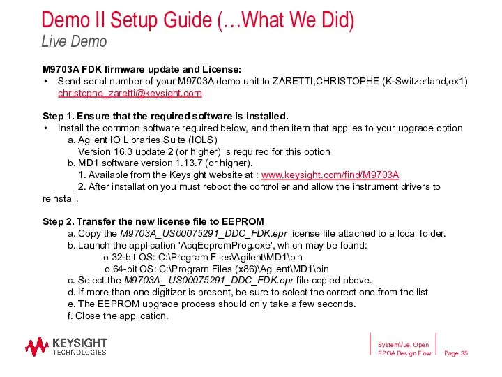
- 35. SystemVue, Open FPGA Design Flow Demo II Setup Guide (…What We Did) Live Demo M9703A FDK
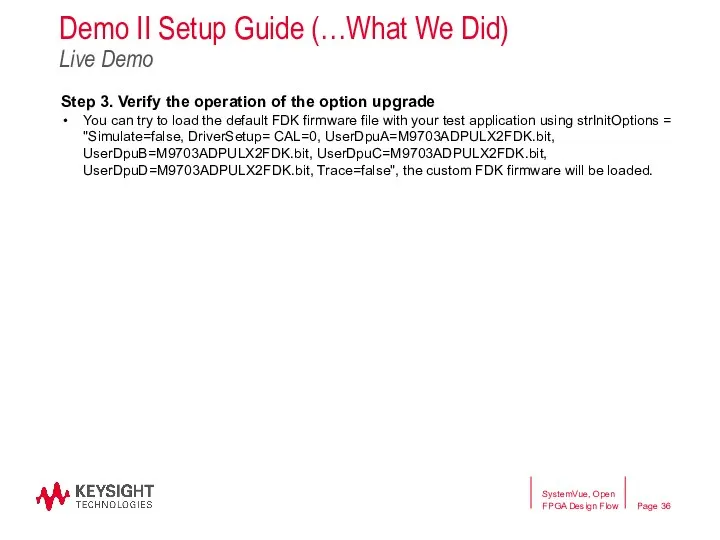
- 36. SystemVue, Open FPGA Design Flow Demo II Setup Guide (…What We Did) Live Demo Step 3.
- 37. SystemVue, Open FPGA Design Flow Realistic Digitizer Application Example Phase & magnitude correction for multi-channel digitizer
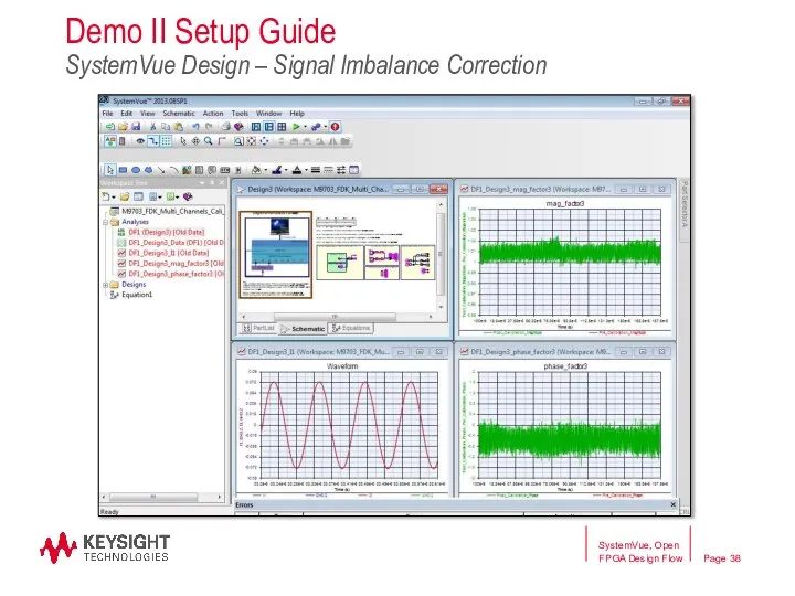
- 38. Demo II Setup Guide SystemVue Design – Signal Imbalance Correction SystemVue, Open FPGA Design Flow
- 39. SystemVue, Open FPGA Design Flow Demo II Setup Guide SystemVue Design – Top Level Workspace
- 40. Demo II Setup Guide SystemVue Design – Chassis Configuration (+External Splitter) SystemVue, Open FPGA Design Flow
- 41. Demo II Setup Guide SystemVue Design – M9703A Configuration SystemVue, Open FPGA Design Flow
- 42. SystemVue, Open FPGA Design Flow Demo II Setup Guide SystemVue Design – 5 Step Signal Correction
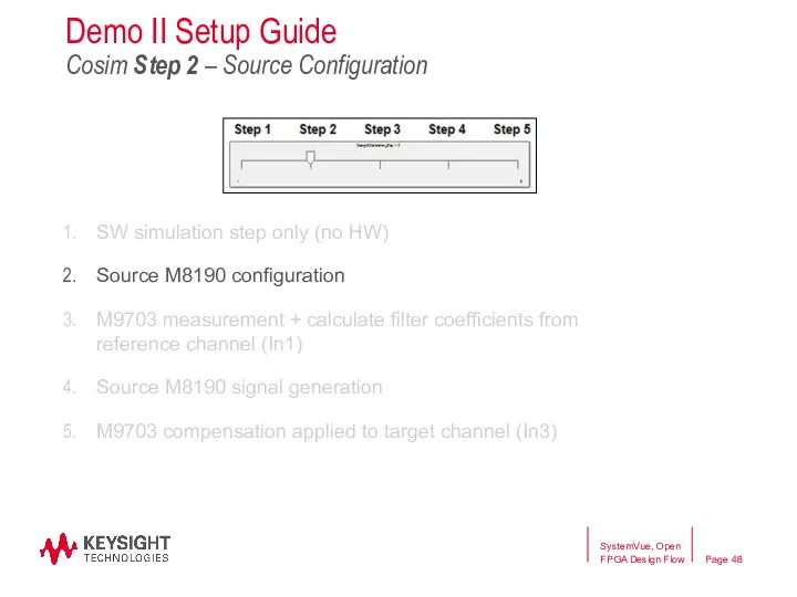
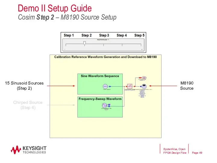
- 43. SW simulation step only (no HW) Source M8190 configuration M9703 measurement + calculate filter coefficients from
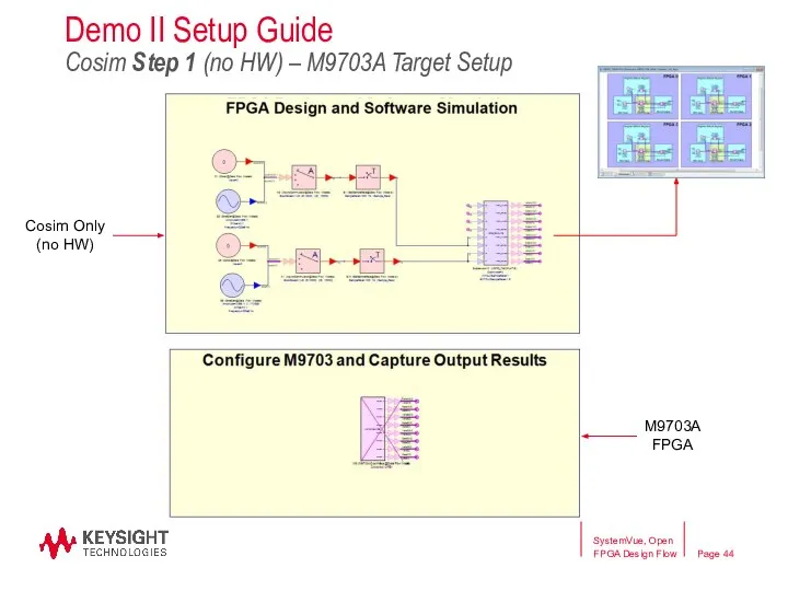
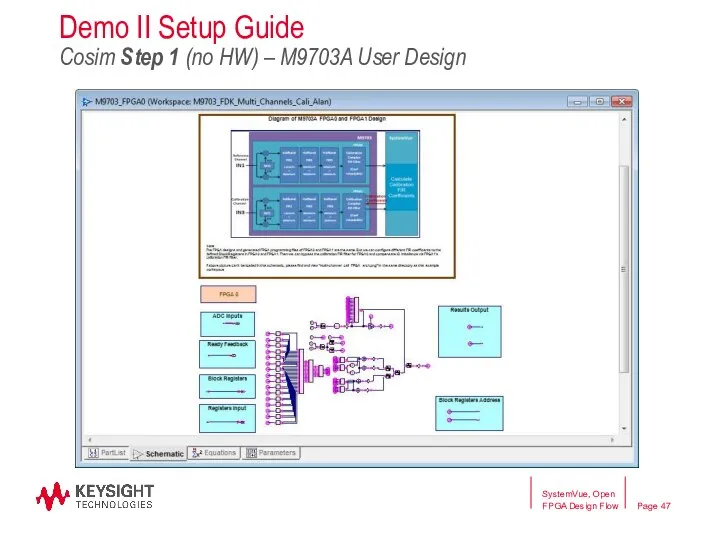
- 44. Demo II Setup Guide Cosim Step 1 (no HW) – M9703A Target Setup SystemVue, Open FPGA
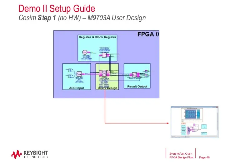
- 45. SystemVue, Open FPGA Design Flow Demo II Setup Guide Cosim Step 1 (no HW) – M9703A
- 46. SystemVue, Open FPGA Design Flow Demo II Setup Guide Cosim Step 1 (no HW) – M9703A
- 47. SystemVue, Open FPGA Design Flow Demo II Setup Guide Cosim Step 1 (no HW) – M9703A
- 48. SW simulation step only (no HW) Source M8190 configuration M9703 measurement + calculate filter coefficients from
- 49. SystemVue, Open FPGA Design Flow Demo II Setup Guide Cosim Step 2 – M8190 Source Setup
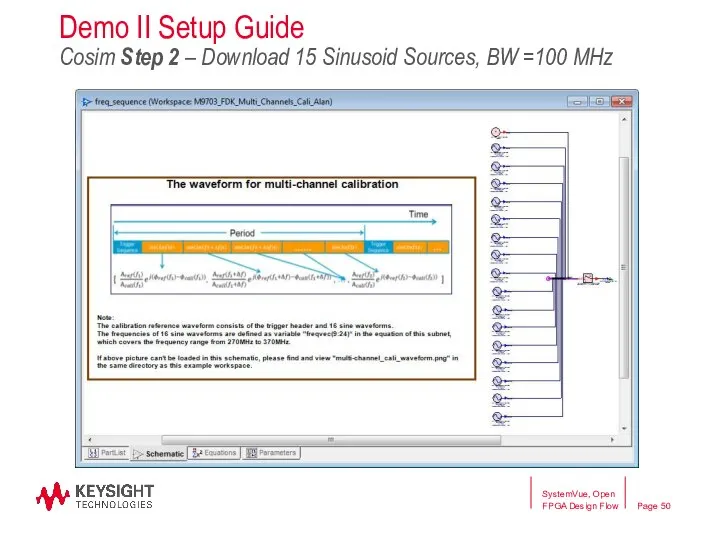
- 50. SystemVue, Open FPGA Design Flow Demo II Setup Guide Cosim Step 2 – Download 15 Sinusoid
- 51. M8190A Secondary Address 60005 (Cleared) SystemVue, Open FPGA Design Flow Demo II Setup Guide Cosim Step
- 52. SystemVue, Open FPGA Design Flow M8190A Primary Address 127.0.0.1 (Error) M8190A Secondary Address 60005 (Cleared) Demo
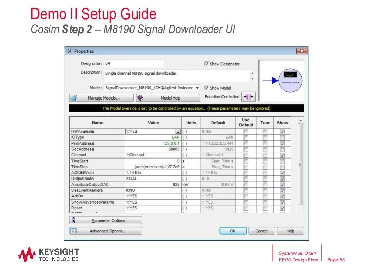
- 53. SystemVue, Open FPGA Design Flow Demo II Setup Guide Cosim Step 2 – M8190 Signal Downloader
- 54. SW simulation step only (no HW) Source M8190 configuration M9703 measurement + calculate filter coefficients from
- 55. M9703 Cosim Parameters M9703 Connection and Options SystemVue, Open FPGA Design Flow Demo II Setup Guide
- 56. SystemVue, Open FPGA Design Flow Demo II Setup Guide Cosim Step 3 – Reference Channel (In1)
- 57. Demo II Setup Guide Cosim Step 3 – Reference Channel (In1) Magnitude SystemVue, Open FPGA Design
- 58. Demo II Setup Guide Cosim Step 3 – Reference Channel (In1) Phase SystemVue, Open FPGA Design
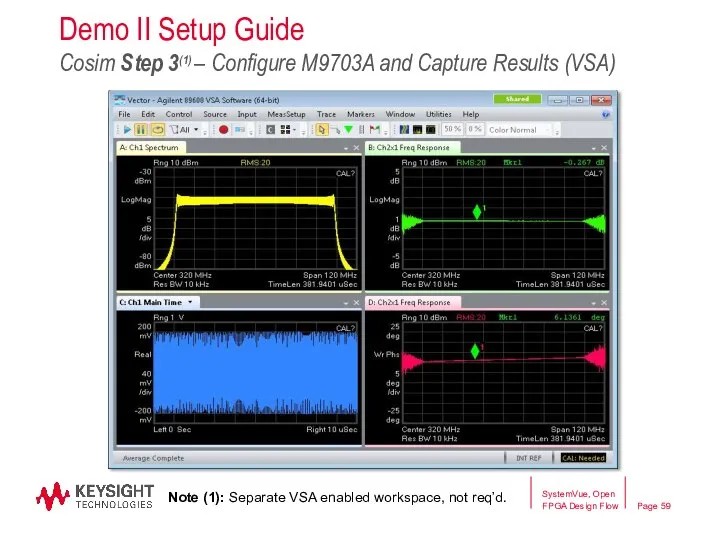
- 59. SystemVue, Open FPGA Design Flow Demo II Setup Guide Cosim Step 3(1) – Configure M9703A and
- 60. SW simulation step only (no HW) Source M8190 configuration M9703 measurement + calculate filter coefficients for
- 61. SystemVue, Open FPGA Design Flow Demo II Setup Guide Cosim Step 4 – M8190 Source Setup
- 62. SW simulation step only (no HW) Source M8190 configuration M9703 measurement + calculate filter coefficients for
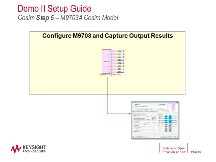
- 63. SystemVue, Open FPGA Design Flow Demo II Setup Guide Cosim Step 5 – M9703A Cosim Model
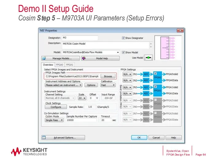
- 64. SystemVue, Open FPGA Design Flow Demo II Setup Guide Cosim Step 5 – M9703A UI Parameters
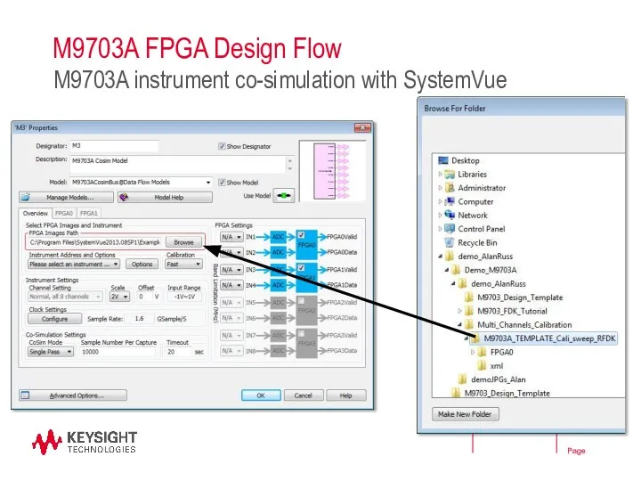
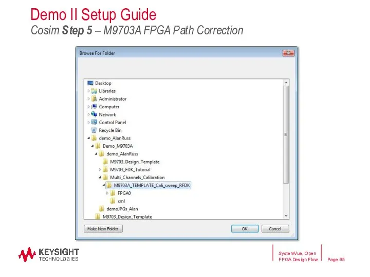
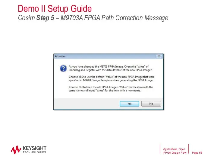
- 65. SystemVue, Open FPGA Design Flow Demo II Setup Guide Cosim Step 5 – M9703A FPGA Path
- 66. SystemVue, Open FPGA Design Flow Demo II Setup Guide Cosim Step 5 – M9703A FPGA Path
- 67. SystemVue, Open FPGA Design Flow Default Path (Error) User Path (Cleared) Note: Drive letter must be
- 68. SystemVue, Open FPGA Design Flow Demo II Setup Guide Cosim Step 5 – M9703A FPGA Setup
- 69. SystemVue, Open FPGA Design Flow Demo II Setup Guide Cosim Step 5 – M9703A FPGA(0) Programming
- 70. SystemVue, Open FPGA Design Flow Demo II Setup Guide Cosim Step 5 – M9703A FPGA(1) Programming
- 71. Demo II Setup Guide Cosim Step 5 – Corrected Channel (In3) Magnitude SystemVue, Open FPGA Design
- 72. Demo II Setup Guide Cosim Step 5 – Corrected Channel (In3) Phase SystemVue, Open FPGA Design
- 73. SystemVue, Open FPGA Design Flow Demo II Setup Guide Cosim Step 5(1) – Configure M9703A and
- 74. Summary Introduction to SystemVue hardware design kit General SystemVue hardware design flow Integrated FPGA design flow
- 75. Thank you Questions yahia_tachwali@keysight.com SystemVue/FPGA Flow
- 76. Backup SystemVue/FPGA Flow
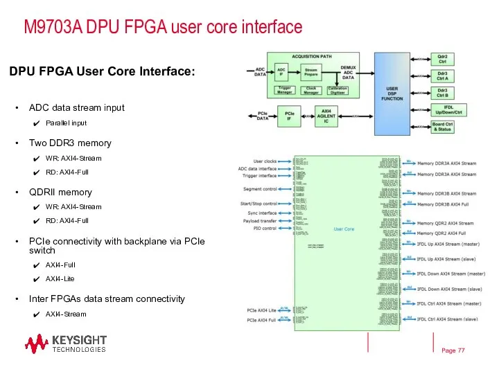
- 77. M9703A DPU FPGA user core interface DPU FPGA User Core Interface: ADC data stream input Parallel
- 78. Early development of Firmware/Software API’s Before HW arrives ADC ADC Register Block Reg DDR MEM DDR
- 79. Standard Conforming Baseband Stimulus and response metrology Available with W1461BP core environment SystemVue “Baseband Verification” Libraries
- 80. Simplify complex post analysis Fixed to floating point data conversion FFT, Filtering, Re-sampling Time / Frequency
- 81. Overcome function test limitation of a timing based simulator Traditional analog functions are being moved to
- 82. Real world system level simulation Digital I/Q BB Modulation Demod & BER TCP/IP client and data
- 84. Скачать презентацию
Hardware Design Using SystemVue
SystemVue, Open FPGA Design Flow
HDL Files
IP
Graphical Design Entry
Textual/Binary
Hardware Design Using SystemVue
SystemVue, Open FPGA Design Flow
HDL Files
IP
Graphical Design Entry
Textual/Binary
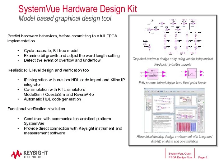
SystemVue Hardware Design Kit
Model based graphical design tool
Predict hardware behaviors, before
SystemVue Hardware Design Kit
Model based graphical design tool
Predict hardware behaviors, before
PART I: SystemVue Open FPGA Design Flow
SystemVue, Open FPGA Design Flow
PART I: SystemVue Open FPGA Design Flow
SystemVue, Open FPGA Design Flow
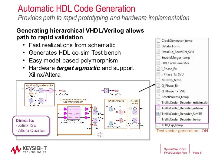
Automatic HDL Code Generation
Provides path to rapid prototyping and hardware implementation
Automatic HDL Code Generation Provides path to rapid prototyping and hardware implementation
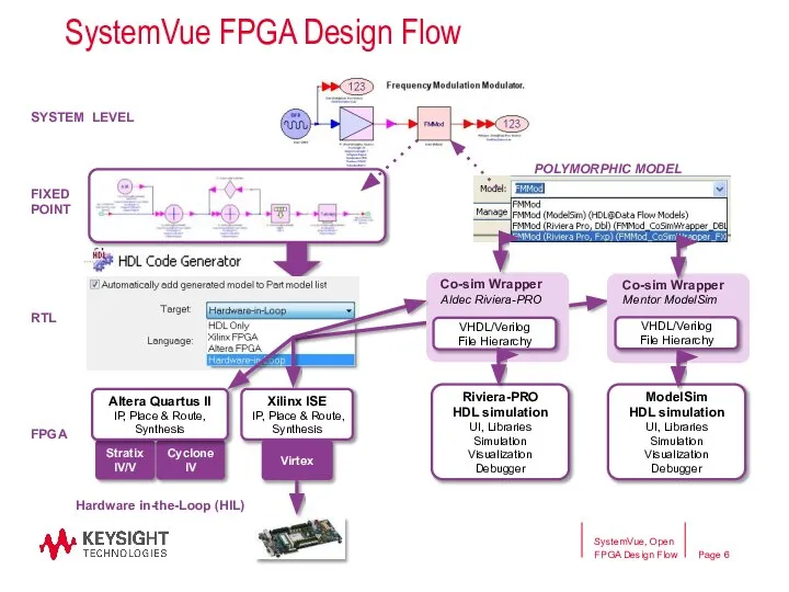
SystemVue FPGA Design Flow
SYSTEM LEVEL
SystemVue, Open FPGA Design Flow
SystemVue FPGA Design Flow
SYSTEM LEVEL
SystemVue, Open FPGA Design Flow
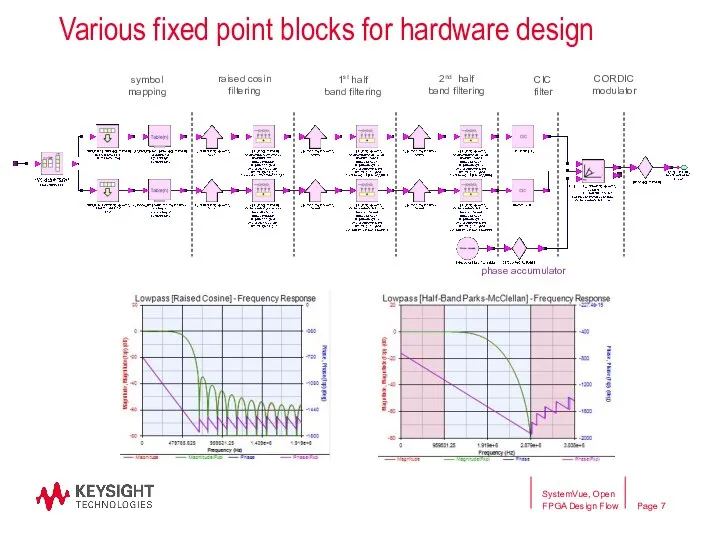
Various fixed point blocks for hardware design
symbol mapping
1st half
band filtering
CIC
filter
CORDIC
modulator
phase accumulator
2nd
Various fixed point blocks for hardware design
symbol mapping
1st half
band filtering
CIC
filter
CORDIC
modulator
phase accumulator
2nd
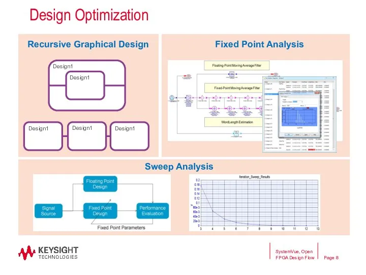
Design Optimization
Fixed Point Analysis
Sweep Analysis
Recursive Graphical Design
Design1
Design1
Design1
Design1
Design1
SystemVue, Open FPGA Design Flow
Design Optimization
Fixed Point Analysis
Sweep Analysis
Recursive Graphical Design
Design1
Design1
Design1
Design1
Design1
SystemVue, Open FPGA Design Flow
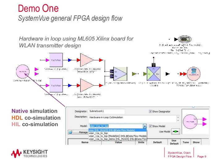
Demo One
SystemVue general FPGA design flow
Native simulation
HDL co-simulation
HIL co-simulation
Hardware
Demo One
SystemVue general FPGA design flow
Native simulation
HDL co-simulation
HIL co-simulation
Hardware
PART II: Integrated Design Flow for M9703A Digitizer
SystemVue, Open FPGA Design
PART II: Integrated Design Flow for M9703A Digitizer
SystemVue, Open FPGA Design
Integrated Hardware Design Flow for Digitizer
Realization of rapid real-time application development
Integrated Hardware Design Flow for Digitizer
Realization of rapid real-time application development
Key Benefits of the integrated design flow
Early development of Firmware/Software APIs
Key Benefits of the integrated design flow
Early development of Firmware/Software APIs
Overview of M9703A High Speed Digitizer
SystemVue/FPGA Flow
8 phase-coherent channels (4 when
Overview of M9703A High Speed Digitizer
SystemVue/FPGA Flow
8 phase-coherent channels (4 when
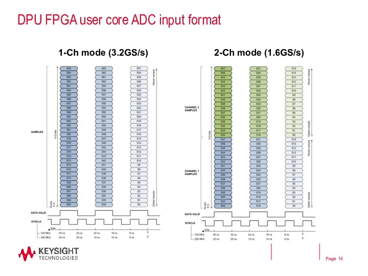
DPU FPGA user core ADC input format
1-Ch mode (3.2GS/s) 2-Ch
DPU FPGA user core ADC input format
1-Ch mode (3.2GS/s) 2-Ch
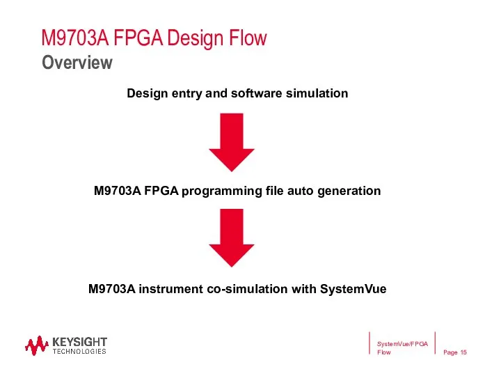
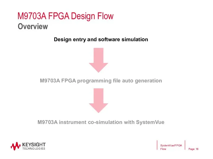
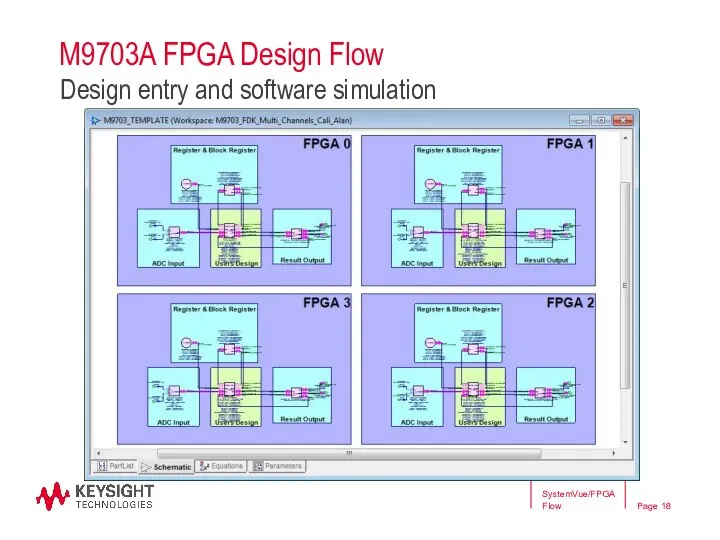
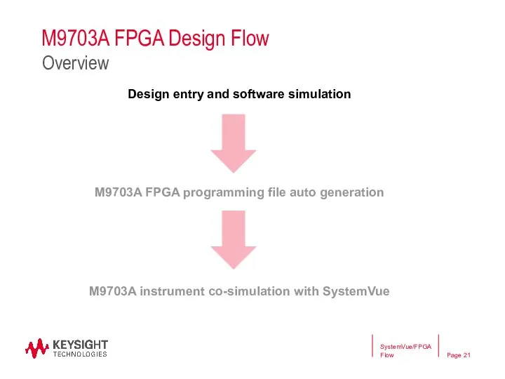
M9703A FPGA Design Flow
Design entry and software simulation
M9703A FPGA programming file
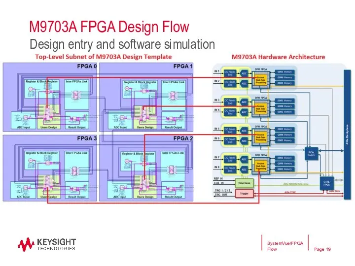
M9703A FPGA Design Flow
Design entry and software simulation
M9703A FPGA programming file
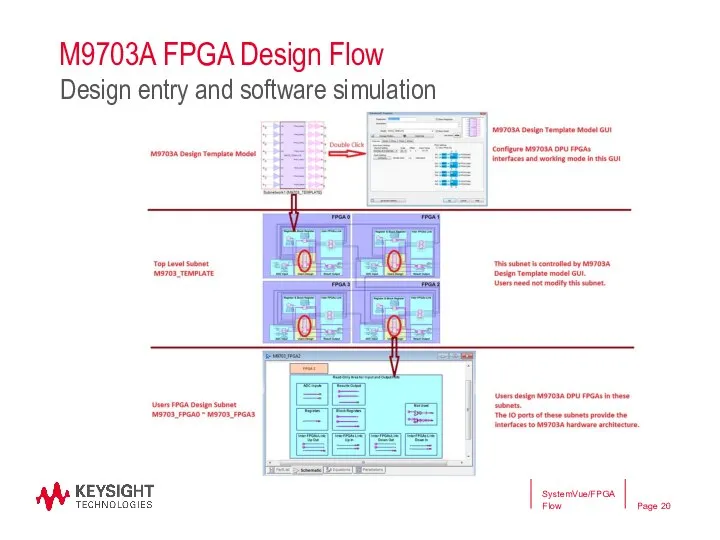
M9703A FPGA Design Flow
Design entry and software simulation
M9703A FPGA programming file
M9703A FPGA Design Flow
Design entry and software simulation
M9703A FPGA programming file
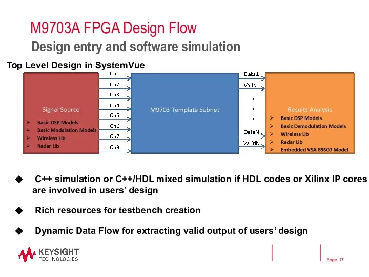
M9703A FPGA Design Flow
C++ simulation or C++/HDL mixed simulation if
M9703A FPGA Design Flow
C++ simulation or C++/HDL mixed simulation if
M9703A FPGA Design Flow
SystemVue/FPGA Flow
Design entry and software simulation
M9703A FPGA Design Flow
SystemVue/FPGA Flow
Design entry and software simulation
M9703A FPGA Design Flow
SystemVue/FPGA Flow
Design entry and software simulation
M9703A FPGA Design Flow
SystemVue/FPGA Flow
Design entry and software simulation
M9703A FPGA Design Flow
SystemVue/FPGA Flow
Design entry and software simulation
M9703A FPGA Design Flow
SystemVue/FPGA Flow
Design entry and software simulation
M9703A FPGA Design Flow
Design entry and software simulation
M9703A FPGA programming file
M9703A FPGA Design Flow
Design entry and software simulation
M9703A FPGA programming file
M9703A FPGA Design Flow
Design entry and software simulation
M9703A FPGA programming file
M9703A FPGA Design Flow
Design entry and software simulation
M9703A FPGA programming file
M9703A FPGA Design Flow
M9703A FPGA programming file auto generation
SystemVue/FPGA Flow
Auto HDL
M9703A FPGA Design Flow
M9703A FPGA programming file auto generation
SystemVue/FPGA Flow
Auto HDL

M9703A FPGA Design Flow
Design entry and software simulation
M9703A FPGA programming file
M9703A FPGA Design Flow
Design entry and software simulation
M9703A FPGA programming file
M9703A FPGA Design Flow
Design entry and software simulation
M9703A FPGA programming file
M9703A FPGA Design Flow
Design entry and software simulation
M9703A FPGA programming file
M9703A FPGA Design Flow
SystemVue/FPGA Flow
M9703A instrument co-simulation with SystemVue
M9703 Cosim Model
M9703
M9703A FPGA Design Flow
SystemVue/FPGA Flow
M9703A instrument co-simulation with SystemVue
M9703 Cosim Model
M9703
M9703A FPGA Design Flow
M9703A instrument co-simulation with SystemVue
M9703A FPGA Design Flow
M9703A instrument co-simulation with SystemVue
M9703A FPGA Design Flow
M9703A instrument co-simulation with SystemVue
M9703A FPGA Design Flow
M9703A instrument co-simulation with SystemVue
Realistic Digitizer Application Example
Phase & magnitude correction for multi-channel digitizer
AD
DDC
FIR
W
Φ
∑
AD
DDC
FIR
W
Φ
AD
DDC
FIR
W
Φ
AD
DDC
FIR
W
Φ
Adaptive Algorithm
I
Q
BEAMS
FPGA
RF
Realistic Digitizer Application Example
Phase & magnitude correction for multi-channel digitizer
AD
DDC
FIR
W
Φ
∑
AD
DDC
FIR
W
Φ
AD
DDC
FIR
W
Φ
AD
DDC
FIR
W
Φ
Adaptive Algorithm
I
Q
BEAMS
FPGA
RF
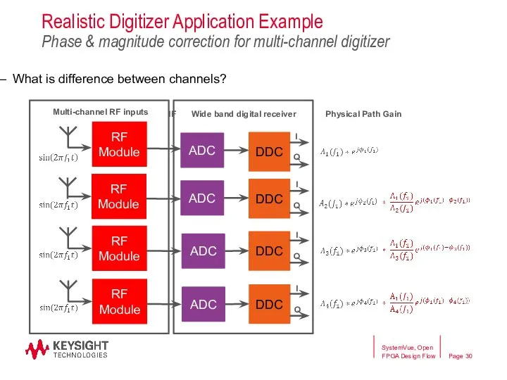
Realistic Digitizer Application Example
Phase & magnitude correction for multi-channel digitizer
What is
Realistic Digitizer Application Example
Phase & magnitude correction for multi-channel digitizer
What is
Realistic Digitizer Application Example
Phase & magnitude correction for multi-channel digitizer
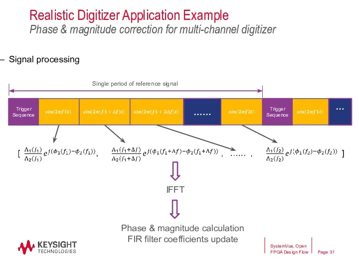
Signal processing
Trigger
Realistic Digitizer Application Example
Phase & magnitude correction for multi-channel digitizer
Signal processing
Trigger
Realistic Digitizer Application Example
Phase & magnitude correction for multi-channel digitizer
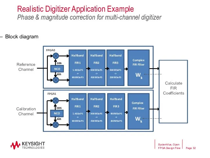
Block diagram
Realistic Digitizer Application Example
Phase & magnitude correction for multi-channel digitizer
Block diagram
SystemVue, Open FPGA Design Flow
Realistic Digitizer Application Example
Phase & magnitude correction
SystemVue, Open FPGA Design Flow
Realistic Digitizer Application Example Phase & magnitude correction
SystemVue, Open FPGA Design Flow
Required Hardware:
M9703 with FDK option to
SystemVue, Open FPGA Design Flow
Required Hardware:
M9703 with FDK option to
SystemVue, Open FPGA Design Flow
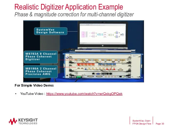
Demo II Setup Guide (…What We Did)
Live
SystemVue, Open FPGA Design Flow
Demo II Setup Guide (…What We Did) Live
SystemVue, Open FPGA Design Flow
Demo II Setup Guide (…What We Did)
Live
SystemVue, Open FPGA Design Flow
Demo II Setup Guide (…What We Did) Live
SystemVue, Open FPGA Design Flow
Realistic Digitizer Application Example
Phase & magnitude correction
SystemVue, Open FPGA Design Flow
Realistic Digitizer Application Example Phase & magnitude correction
Demo II Setup Guide
SystemVue Design – Signal Imbalance Correction
SystemVue, Open
Demo II Setup Guide
SystemVue Design – Signal Imbalance Correction
SystemVue, Open
SystemVue, Open FPGA Design Flow
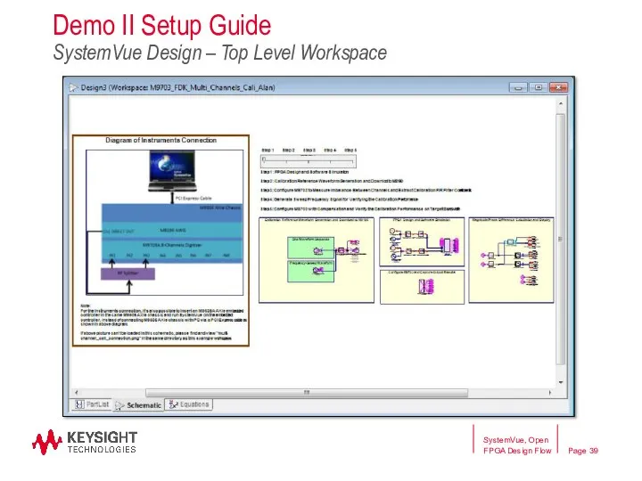
Demo II Setup Guide
SystemVue Design –
SystemVue, Open FPGA Design Flow
Demo II Setup Guide SystemVue Design –
Demo II Setup Guide
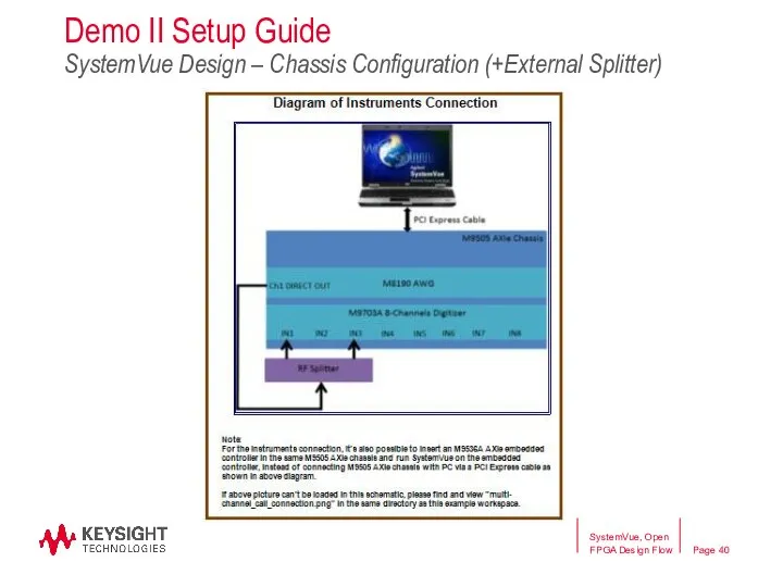
SystemVue Design – Chassis Configuration (+External Splitter)
SystemVue, Open
Demo II Setup Guide
SystemVue Design – Chassis Configuration (+External Splitter)
SystemVue, Open
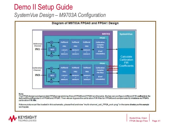
Demo II Setup Guide
SystemVue Design – M9703A Configuration
SystemVue, Open FPGA Design
Demo II Setup Guide
SystemVue Design – M9703A Configuration
SystemVue, Open FPGA Design
SystemVue, Open FPGA Design Flow
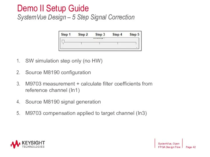
Demo II Setup Guide
SystemVue Design – 5
SystemVue, Open FPGA Design Flow
Demo II Setup Guide SystemVue Design – 5
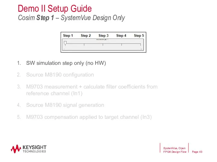
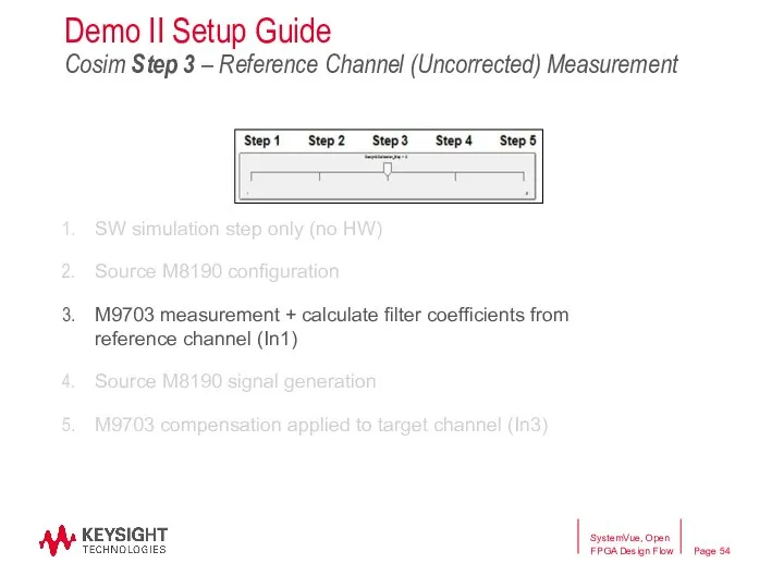
SW simulation step only (no HW)
Source M8190 configuration
M9703 measurement + calculate
SW simulation step only (no HW)
Source M8190 configuration
M9703 measurement + calculate
Demo II Setup Guide
Cosim Step 1 (no HW) – M9703A Target
Demo II Setup Guide Cosim Step 1 (no HW) – M9703A Target
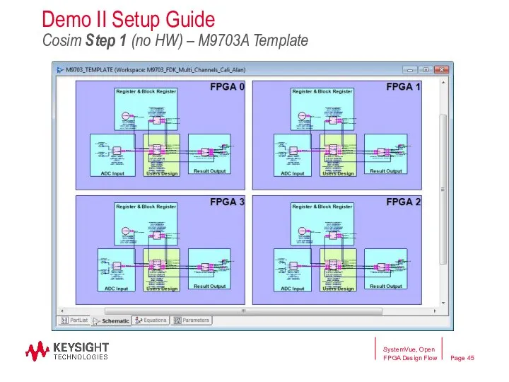
SystemVue, Open FPGA Design Flow
Demo II Setup Guide
Cosim Step 1 (no
SystemVue, Open FPGA Design Flow
Demo II Setup Guide Cosim Step 1 (no
SystemVue, Open FPGA Design Flow
Demo II Setup Guide
Cosim Step 1 (no
SystemVue, Open FPGA Design Flow
Demo II Setup Guide Cosim Step 1 (no
SystemVue, Open FPGA Design Flow
Demo II Setup Guide
Cosim Step 1 (no
SystemVue, Open FPGA Design Flow
Demo II Setup Guide Cosim Step 1 (no
SW simulation step only (no HW)
Source M8190 configuration
M9703 measurement + calculate
SW simulation step only (no HW)
Source M8190 configuration
M9703 measurement + calculate
SystemVue, Open FPGA Design Flow
Demo II Setup Guide
Cosim Step 2 –
SystemVue, Open FPGA Design Flow
Demo II Setup Guide Cosim Step 2 –
SystemVue, Open FPGA Design Flow
Demo II Setup Guide
Cosim Step 2 –
SystemVue, Open FPGA Design Flow
Demo II Setup Guide Cosim Step 2 –
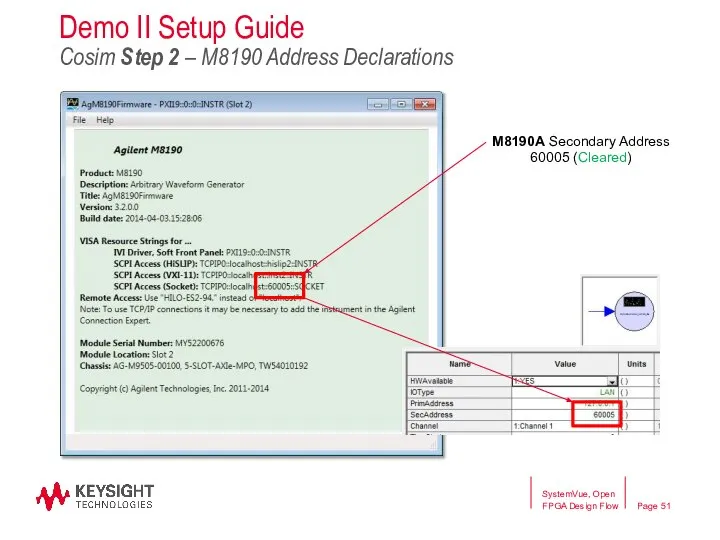
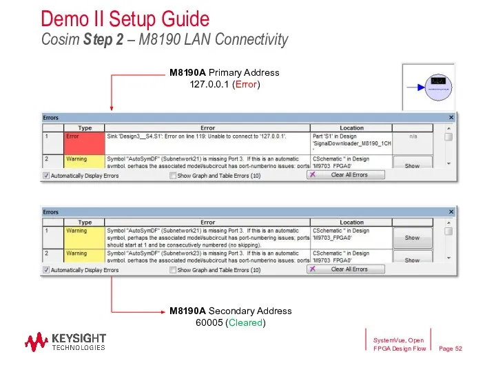
M8190A Secondary Address 60005 (Cleared)
SystemVue, Open FPGA Design Flow
Demo II Setup
M8190A Secondary Address 60005 (Cleared)
SystemVue, Open FPGA Design Flow
Demo II Setup
SystemVue, Open FPGA Design Flow
M8190A Primary Address
127.0.0.1 (Error)
M8190A Secondary Address
SystemVue, Open FPGA Design Flow
M8190A Primary Address
127.0.0.1 (Error)
M8190A Secondary Address
SystemVue, Open FPGA Design Flow
Demo II Setup Guide
Cosim Step 2 –
SystemVue, Open FPGA Design Flow
Demo II Setup Guide Cosim Step 2 –
SW simulation step only (no HW)
Source M8190 configuration
M9703 measurement + calculate
SW simulation step only (no HW)
Source M8190 configuration
M9703 measurement + calculate
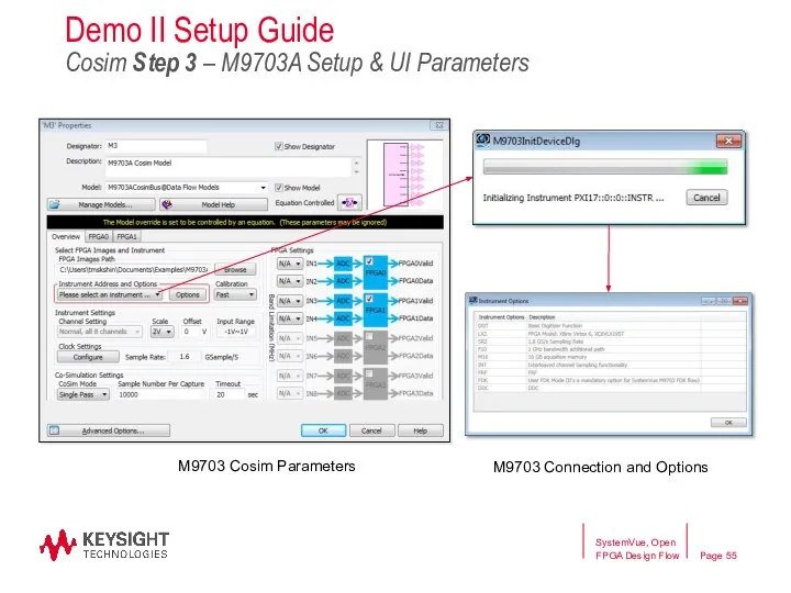
M9703 Cosim Parameters
M9703 Connection and Options
SystemVue, Open FPGA Design Flow
Demo II
M9703 Cosim Parameters
M9703 Connection and Options
SystemVue, Open FPGA Design Flow
Demo II
SystemVue, Open FPGA Design Flow
Demo II Setup Guide
Cosim Step 3 –
SystemVue, Open FPGA Design Flow
Demo II Setup Guide Cosim Step 3 –
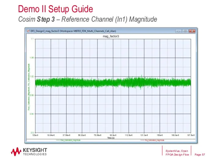
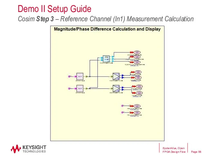
Demo II Setup Guide
Cosim Step 3 – Reference Channel (In1) Magnitude
SystemVue,
Demo II Setup Guide
Cosim Step 3 – Reference Channel (In1) Magnitude
SystemVue,
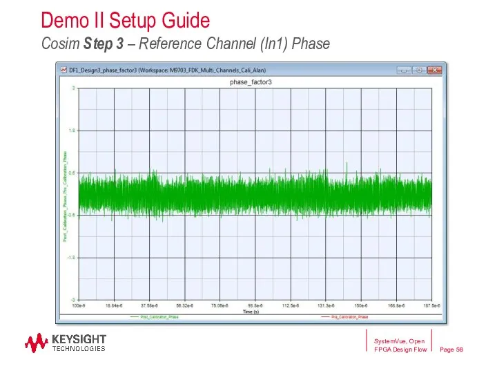
Demo II Setup Guide
Cosim Step 3 – Reference Channel (In1) Phase
SystemVue,
Demo II Setup Guide
Cosim Step 3 – Reference Channel (In1) Phase
SystemVue,
SystemVue, Open FPGA Design Flow
Demo II Setup Guide
Cosim Step 3(1) –
SystemVue, Open FPGA Design Flow
Demo II Setup Guide Cosim Step 3(1) –
SW simulation step only (no HW)
Source M8190 configuration
M9703 measurement + calculate
SW simulation step only (no HW)
Source M8190 configuration
M9703 measurement + calculate
SystemVue, Open FPGA Design Flow
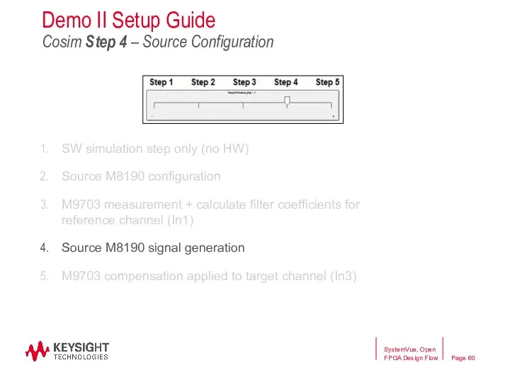
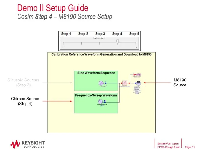
Demo II Setup Guide
Cosim Step 4 –
SystemVue, Open FPGA Design Flow
Demo II Setup Guide Cosim Step 4 –
SW simulation step only (no HW)
Source M8190 configuration
M9703 measurement + calculate
SW simulation step only (no HW)
Source M8190 configuration
M9703 measurement + calculate
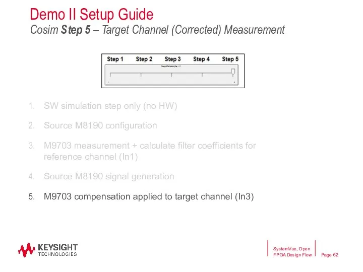
SystemVue, Open FPGA Design Flow
Demo II Setup Guide
Cosim Step 5 –
SystemVue, Open FPGA Design Flow
Demo II Setup Guide Cosim Step 5 –
SystemVue, Open FPGA Design Flow
Demo II Setup Guide
Cosim Step 5 –
SystemVue, Open FPGA Design Flow
Demo II Setup Guide Cosim Step 5 –
SystemVue, Open FPGA Design Flow
Demo II Setup Guide
Cosim Step 5 –
SystemVue, Open FPGA Design Flow
Demo II Setup Guide Cosim Step 5 –
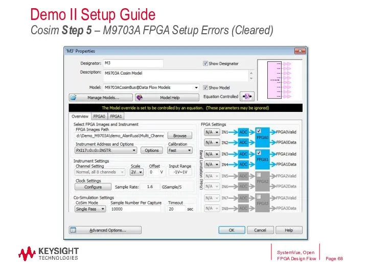
SystemVue, Open FPGA Design Flow
Demo II Setup Guide
Cosim Step 5 –
SystemVue, Open FPGA Design Flow
Demo II Setup Guide Cosim Step 5 –
SystemVue, Open FPGA Design Flow
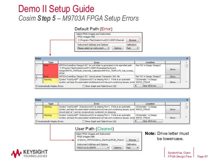
Default Path (Error)
User Path (Cleared)
Note: Drive letter
SystemVue, Open FPGA Design Flow
Default Path (Error)
User Path (Cleared)
Note: Drive letter
SystemVue, Open FPGA Design Flow
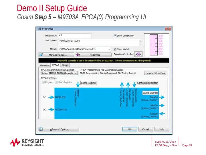
Demo II Setup Guide
Cosim Step 5 –
SystemVue, Open FPGA Design Flow
Demo II Setup Guide Cosim Step 5 –
SystemVue, Open FPGA Design Flow
Demo II Setup Guide
Cosim Step 5 –
SystemVue, Open FPGA Design Flow
Demo II Setup Guide Cosim Step 5 –

SystemVue, Open FPGA Design Flow
Demo II Setup Guide
Cosim Step 5 –
SystemVue, Open FPGA Design Flow
Demo II Setup Guide Cosim Step 5 –
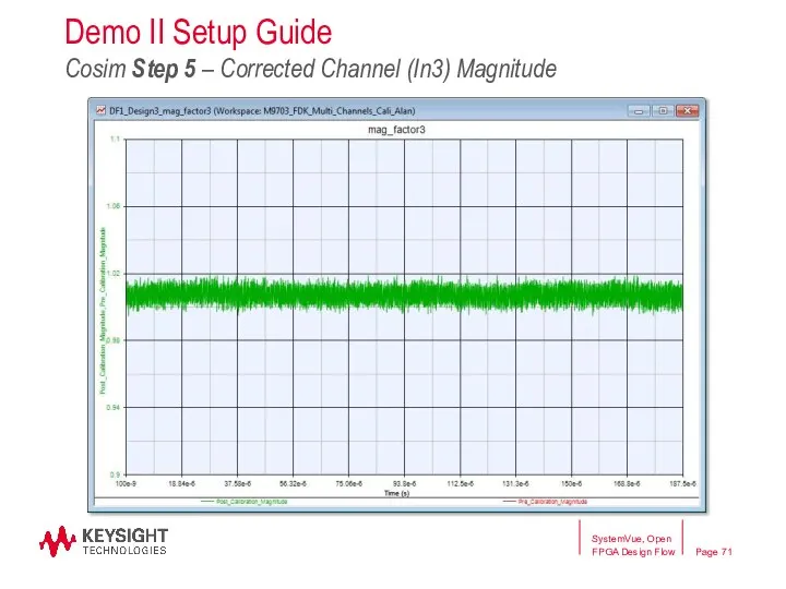
Demo II Setup Guide
Cosim Step 5 – Corrected Channel (In3) Magnitude
SystemVue,
Demo II Setup Guide
Cosim Step 5 – Corrected Channel (In3) Magnitude
SystemVue,
Demo II Setup Guide
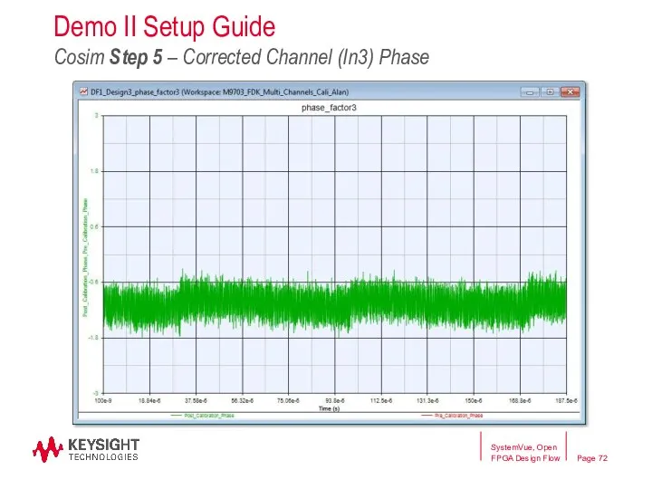
Cosim Step 5 – Corrected Channel (In3) Phase
SystemVue,
Demo II Setup Guide
Cosim Step 5 – Corrected Channel (In3) Phase
SystemVue,
SystemVue, Open FPGA Design Flow
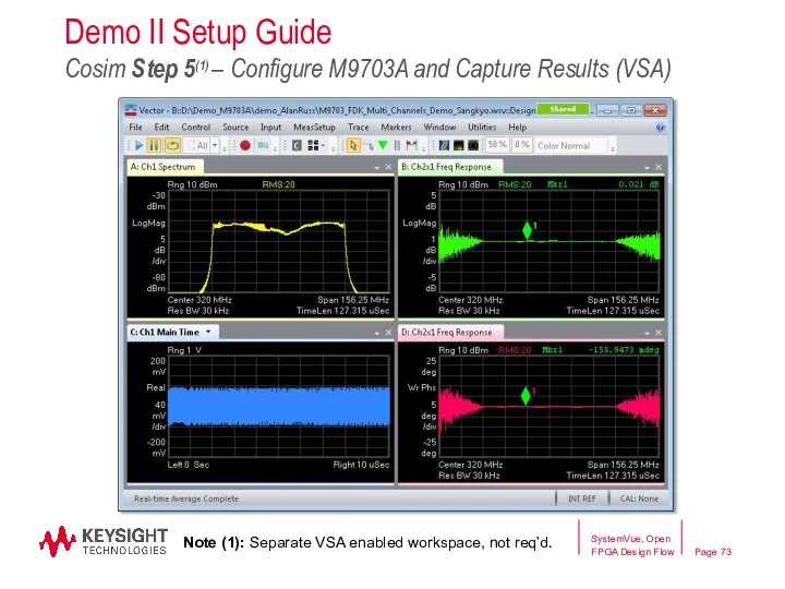
Demo II Setup Guide
Cosim Step 5(1) –
SystemVue, Open FPGA Design Flow
Demo II Setup Guide Cosim Step 5(1) –
Summary
Introduction to SystemVue hardware design kit
General SystemVue hardware design flow
Integrated FPGA
Summary
Introduction to SystemVue hardware design kit
General SystemVue hardware design flow
Integrated FPGA
Thank you
Questions
yahia_tachwali@keysight.com
SystemVue/FPGA Flow
Thank you
Questions
yahia_tachwali@keysight.com
SystemVue/FPGA Flow
Backup
SystemVue/FPGA Flow
Backup
SystemVue/FPGA Flow
M9703A DPU FPGA user core interface
DPU FPGA User Core Interface:
ADC
M9703A DPU FPGA user core interface
DPU FPGA User Core Interface:
ADC
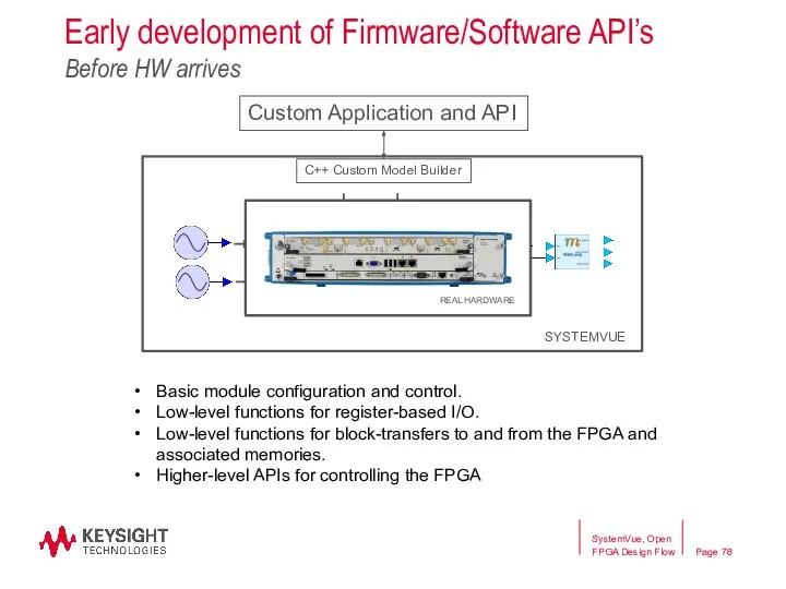
Early development of Firmware/Software API’s
Before HW arrives
ADC
ADC
Register
Block Reg
DDR MEM
DDR MEM
FPGA
M9703_TEMPLATE
SYSTEMVUE
Basic module
Early development of Firmware/Software API’s
Before HW arrives
ADC
ADC
Register
Block Reg
DDR MEM
DDR MEM
FPGA
M9703_TEMPLATE
SYSTEMVUE
Basic module
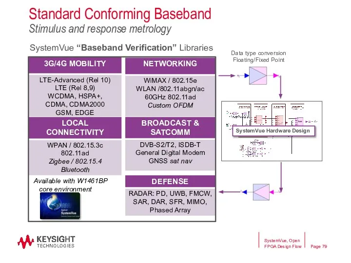
Standard Conforming Baseband
Stimulus and response metrology
Available with W1461BP
core environment
SystemVue
Standard Conforming Baseband
Stimulus and response metrology
Available with W1461BP
core environment
SystemVue
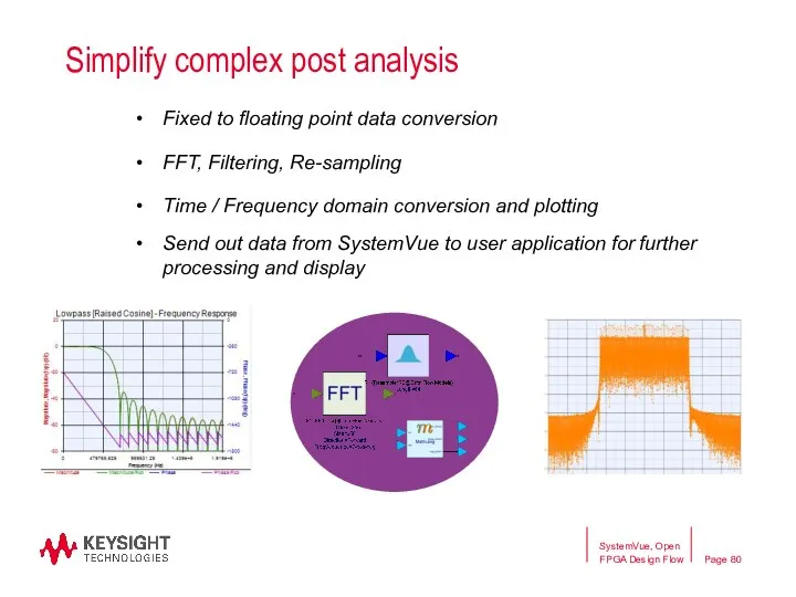
Simplify complex post analysis
Fixed to floating point data conversion
FFT, Filtering, Re-sampling
Time
Simplify complex post analysis
Fixed to floating point data conversion
FFT, Filtering, Re-sampling
Time
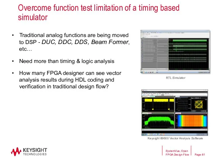
Overcome function test limitation of a timing based simulator
Traditional analog functions
Overcome function test limitation of a timing based simulator
Traditional analog functions
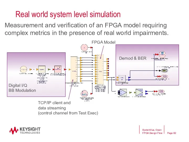
Real world system level simulation
Digital I/Q
BB Modulation
Demod & BER
TCP/IP client
Real world system level simulation
Digital I/Q
BB Modulation
Demod & BER
TCP/IP client
 Шаблон лабораторной работы. Наименование проектной инициативы
 Литературная игра Загадки Василисы Премудрой
 Есть ли жизнь без интернета?
 Strategy Russian Corporate Bonds
 Розробка та дослідження екструзійного преса з стабілізованою швидкістю бруса для виробництва будівельної кераміки
 Planificarea activitatilor de transport. Curs 3
 ADX Interfaces Architecture MOB
 Седло для Пегаса
 Разработка технологии датчиков и их запуск
 Загальні питання про технологічне обладнання для виготовлення взуття
 Клинский_частный дом_г.о.Клин, д. Колосово_схема
 Английский .Брест
 Возникновение Ислама. Арабские завоевания
 Технические средства информатизации. Системные платы
 Синквейны Венцловский
 Ты моя звездочка
 Лучший по профессии работник ОАО Белинвестбанк
 Число теоретических тарелок
 Неделя Всех Святых
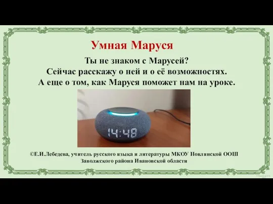 Умная Маруся
 ВКР в электронном формате в ЭИОС Университета
 Атмосфера подготовки к Новому году в живописи
 Chall-2_p73
 20120507_vystuplenie_pr
 Битумные эмульсии, вязкий битум и битумно-резиновые дисперсии, дегтевые материалы
 Курс 3 Занятие 2
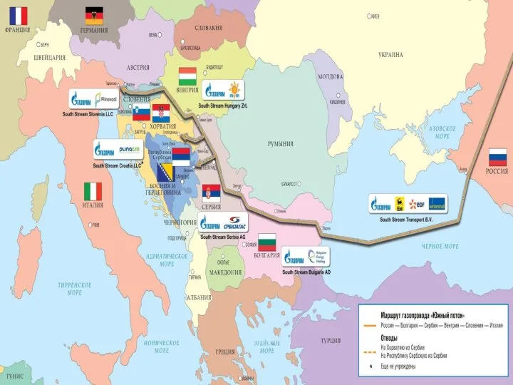 Маршрут газопровода Южный поток
 Зимующие птицы