- Optical identification using imperfections in 2D materials

Содержание
- 2. Introduction The ability to uniquely identify an object or device is important for authentication. Imperfections, locked
- 4. Objective To analise a proposed simple optical technique to read unique information from nanometer-scale defects in
- 5. Tasks Method Results for WS2 from mechanically exfoliation Results for WS2 from chemical vapor deposition Conclusion
- 6. Method Measurement apparatus, in which the photoluminescence from a monolayer TMD is collected by an objective
- 7. Angular orientations of the BPF determines the center-wavelength of its pass band, which varies with incidence
- 8. Concept of the angular selective transmission Changing the BPF angle lights up a random subset of
- 9. Makeup of PUF The BPF angular orientation θ, the corresponding BPF bandwidth, and the spatially varying
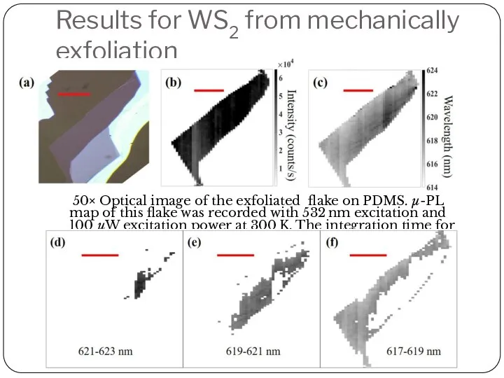
- 10. Results for WS2 from mechanically exfoliation 50× Optical image of the exfoliated flake on PDMS. μ-PL
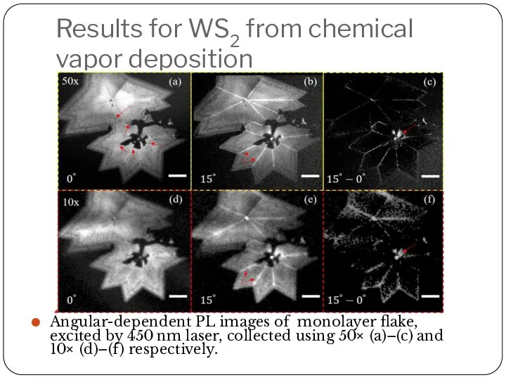
- 11. Results for WS2 from chemical vapor deposition Angular-dependent PL images of monolayer flake, excited by 450
- 12. Angular dependent PL images of WS2 monolayer flake, excited by 450 nm laser, imaged by a
- 14. Скачать презентацию
Introduction
The ability to uniquely identify an object or device is important
Introduction
The ability to uniquely identify an object or device is important
Objective
To analise a proposed simple optical technique to read unique information from
Objective
To analise a proposed simple optical technique to read unique information from
Tasks
Method
Results for WS2 from mechanically exfoliation
Results for WS2 from chemical vapor
Tasks
Method
Results for WS2 from mechanically exfoliation
Results for WS2 from chemical vapor
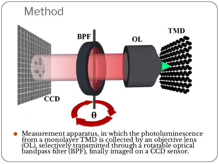
Method
Measurement apparatus, in which the photoluminescence from a monolayer TMD is
Method
Measurement apparatus, in which the photoluminescence from a monolayer TMD is
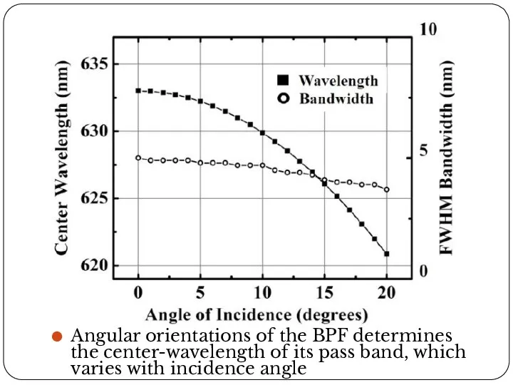
Angular orientations of the BPF determines the center-wavelength of its pass
Angular orientations of the BPF determines the center-wavelength of its pass
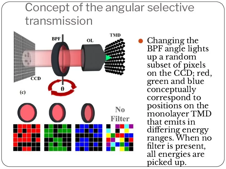
Concept of the angular selective transmission
Changing the BPF angle lights up
Concept of the angular selective transmission
Changing the BPF angle lights up
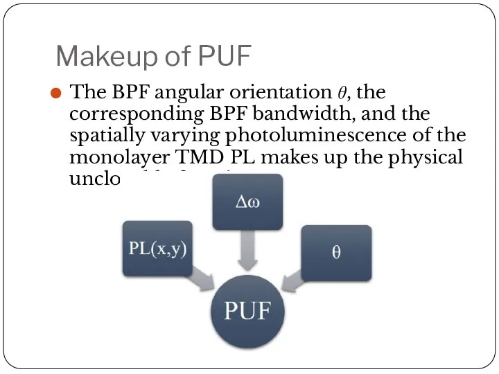
Makeup of PUF
The BPF angular orientation θ, the corresponding BPF bandwidth, and
Makeup of PUF
The BPF angular orientation θ, the corresponding BPF bandwidth, and
Results for WS2 from mechanically exfoliation
50× Optical image of the exfoliated flake
Results for WS2 from mechanically exfoliation
50× Optical image of the exfoliated flake
Results for WS2 from chemical vapor deposition
Angular-dependent PL images of monolayer flake,
Results for WS2 from chemical vapor deposition
Angular-dependent PL images of monolayer flake,
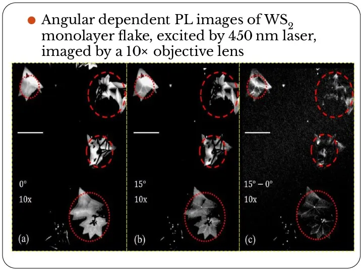
Angular dependent PL images of WS2 monolayer flake, excited by 450 nm
Angular dependent PL images of WS2 monolayer flake, excited by 450 nm
 Масленица Кустодиев Борис Михайлович (1878-1927) (автопортрет) 5 класс Учитель: Перевозникова Е.В.
 ҚР оңтүстік аймақтарын табиғи газбен жабдықтау мәселелері
 Инфекции
 Виды, разрезы, сечения
 Индукционная плита
 Тематический урок русского языка с элементами ПДД.
 В поисках Истины
 Презентация Совет безопасности РФ
 Презентация ООО «Допинг» для Freedom концерт-холл
 Сохранение и популяризация историко-культурного и природного наследия Арктики: возможности компьютерной игры
 Меланоцитарные и нейрогенные опухоли
 правила личной гигиены Выполнила: Замараева Яна Ученица 4 «В» класса МОУ СОШ № 32 Г.Уссурийск 2011 г.
 Liczby w Biblii
 Презентация на тему "Авторская технология взаимодействия участников образовательного процесса при организации системы монито
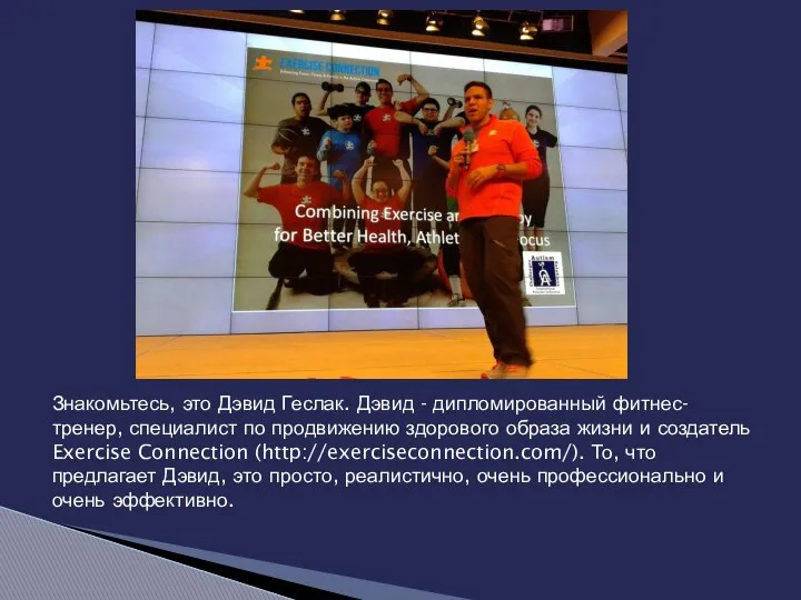 Дэвид Геслак. Упражнения для тренировок с особенными людьми
 Работы победителей муниципального этапа областного конкурса детского и юношеского изобразительного искусства «Я рисую
 Школьная или обычная форма
 Влияние занятий роллер спортом на состояние здоровья детей 10-12 лет
 Презентация Таможенный платежи кроссворд
 Модели сущность-связь
 Презентация Классическое Средневековье (XI -XV вв.)
 ß-адреноблокаторы – величайший прорыв в лечении сердечно-сосудистых заболеваний
 Социально-исторические предпосылки государства и права. Возникновение государства и права
 Страхование ответственности за загрязнение окружающей среды (экологическое страхование) в России и за рубежом
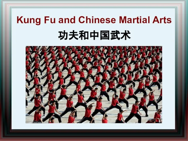 Kung fu and chinese martial arts
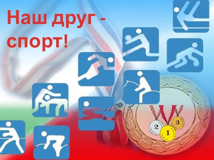 Наш друг - спорт
 Распространенные заболевания человека
 Презентация на тему "Интерактивные методы обучения как фактор мотивации качества учебного материала" - скачать презентации п