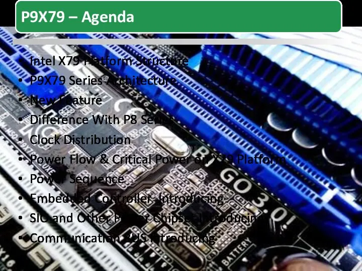
- P9X79 Series Confidential

Содержание
- 2. Intel X79 Platform Structure P9X79 Series Architecture New Feature Difference With P8 Series Clock Distribution Power
- 3. Intel X79 Platform Structure P9X79 Series Architecture New Feature Difference With P8 Series Clock Distribution Power
- 4. CPU 6C/12T, 4C/8T Support PCIe 3.0 DRAM support up to 4ch, 8xDIMM, Max. 64GB Supports NVIDIA®
- 5. Support 8GB,MAX is for 64GB Support DDR3 2400(O.C.)/2133(O.C.) 1866/1600/1333/1066 Support Intel® Extreme Memory Profile(XMP) Support DIGI+
- 6. Intel X79 Platform Structure P9X79 Series Architecture New Feature Difference With P8 Series Clock Distribution Power
- 9. Intel X79 Platform Structure P9X79 Series Architecture New Feature Difference With P8 Series Clock Distribution Power
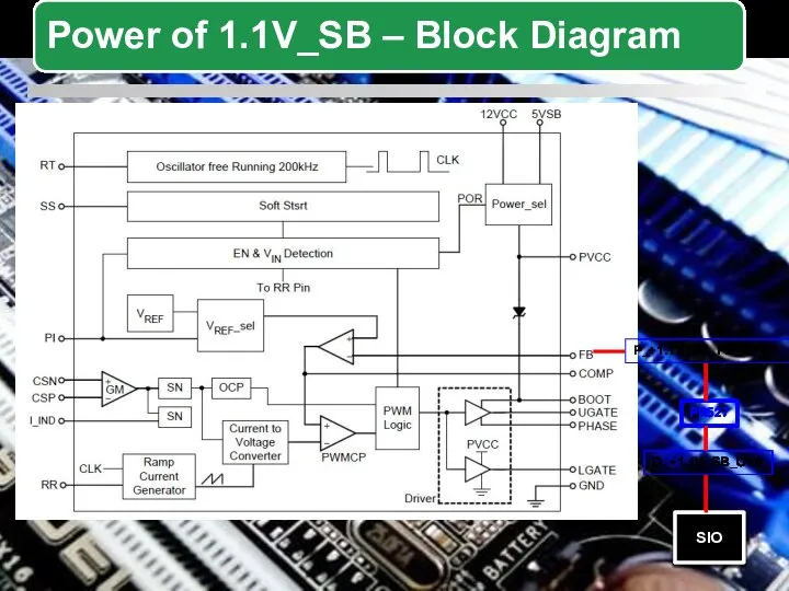
- 10. DIGI+ Power Control (2/6) Most Precise Adjustment on CPU & DRAM Extreme Performance & O.C. Capability
- 11. Smart chip control without boot-up No need to open chassis Complete within only ONE click
- 12. Intel X79 Platform Structure P9X79 Series Architecture New Feature Difference With P8 Series Clock Distribution Power
- 13. DRAM power control: Analog ? DIGITAL Clock Generator: PCH Internal ? External E-SATA support 6G ?
- 14. Analog PWM CONTROLLER UP6203 1.5VDUAL_REF EC phase MOS driver 1.5VDUAL Digital PWM CONTROLLER ASP1101 EC phase
- 15. Intel X79 Platform Structure P9X79 Series Architecture New Feature Difference With P8 Series Clock Distribution Power
- 17. ICS428: SIO, PCI, SATA… ICS1218: CPU, CPU_QPI, DMI, PCIE, PCIE onboard device… ICS1218
- 18. PCIE2.0 USB
- 19. 1218 428 +VTT_CPU_PWRGD CK420_PWRGD# 25 MHz 25 MHz Power Power
- 20. +3VDUAL +VDD_CLK
- 21. 428 CLK GEN 1218 CLK GEN
- 23. Server MB (For C_CPU) SAS Marvall 9128 (SATA) C_PCH_GND (ex: E-SATA)
- 24. Intel X79 Platform Structure P9X79 Series Architecture New Feature Difference With P8 Series Clock Distribution Power
- 29. Intel X79 Platform Structure P9X79 Series Architecture New Feature Difference With P8 Series Clock Distribution Power
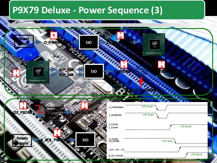
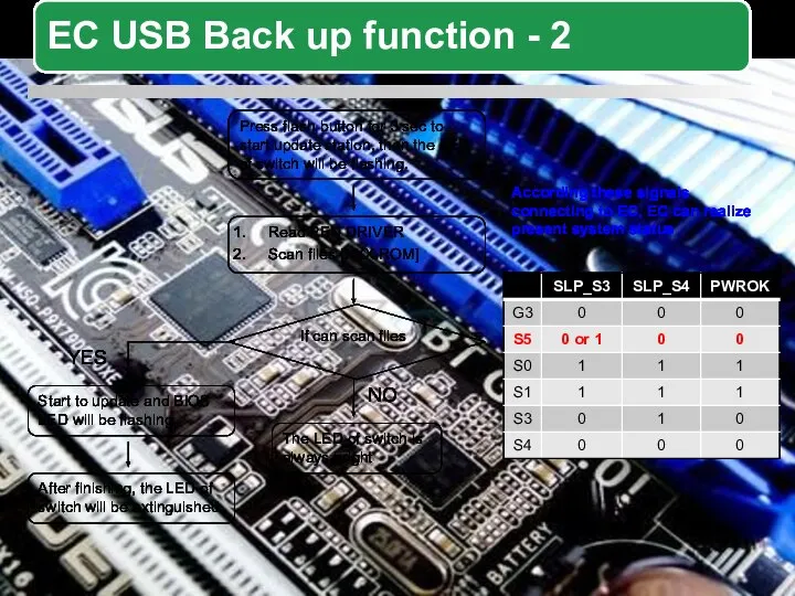
- 30. G3: Battery S0: All Power S3: Standby and Dual Deep S5: Only ATX Power
- 31. (PWRBTN#IN, KB MS Wakeup)
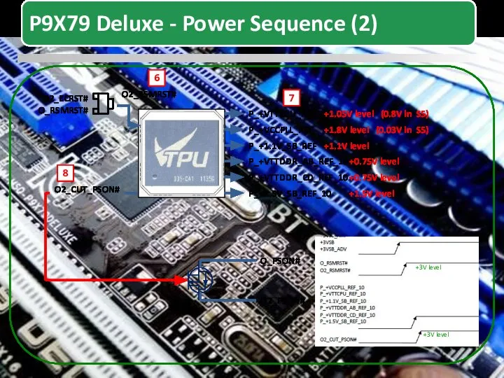
- 33. SIO 3V_ATX +BAT_3V SR88 S_SRTCRST O2_ECRST# Power Supply O_RSMRST# O2_ECRST# O_RSMRST# O2_RSMRST# 1 2 3 4
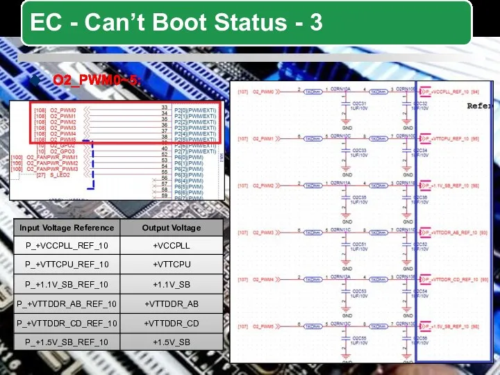
- 34. O2_ECRST# O2_RSMRST# P_+VCCPLL_REF +1.8V level (0.03V in S5) P_+VTTCPU_REF +1.05V level (0.8V in S5) P_+1.1V_SB_REF +1.1V
- 35. SIO Power Button O_PWRBTN#IN O_PWRBTN# SIO SLP_S3# SLP_S4# O_PSON# O2_CUT_PSON# O2_PSON# +3V level +3V level +3V
- 36. +VTT_CPU, +1.5VDUAL_AB, +1.5VDUAL_CD, +1.1V_SB, +1.5V_SB +1.05V level +1.5V level +1.5V level +1.1V level +1.5V level 16
- 37. +VTTCPU => VTT_CPU_PWRGD
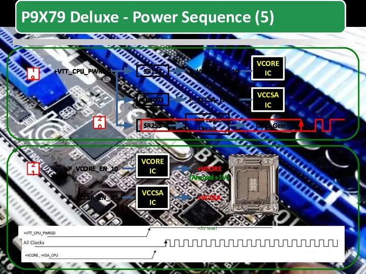
- 38. 19 +VTT_CPU_PWRGD VCORE IC VCCSA IC SR151 SR1003 P_VCORE_EN_10 P_VCCSA_EN_10 SR255 Clock Gen MB Logic Circuit
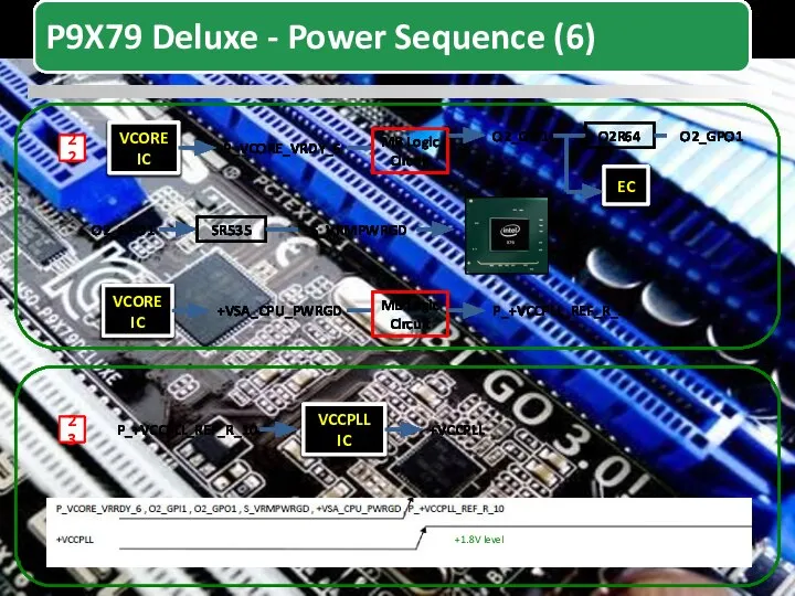
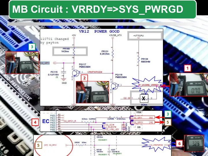
- 39. VCORE IC P_VCORE_VRDY_6 22 O2_GPI1 MB Logic Circuit O2R64 S_VRMPWRGD EC O2_GPO1 SR535 O2_GPO1 +VSA_CPU_PWRGD VCORE
- 40. X 1 2 3 3 EC 5 4 5 6
- 41. +VSA_CPU_PWRGD => P_+VCCPLL_REF_R_10
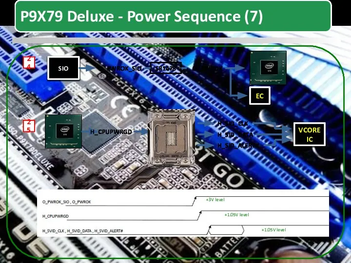
- 42. 24 SIO O_PWROK_SIO EC SR1478 O_PWROK H_CPUPWRGD H_SID_CLK H_SID_DATA H_SID_ALERT# VCORE IC 25 +3V level +1.05V
- 43. S_VRMPWRGD 26 S_PLTRST# SIO LAN Other Devices 27 SIO O_PCIRST#_PCIEX16_* [1:3] MB PCIE S_PLTRST# 28 H_CPURST#
- 44. Intel X79 Platform Structure P9X79 Series Architecture New Feature Difference With P8 Series Clock Distribution Power
- 45. S_PLTRST => H_CPURST# 1 EC 2 3
- 46. EC is a 8051 micro-processor EC functions DIGI+ Power Control--SMBUS interface Over-voltage control, 3.2V/512=6.25mV/step--PWM interface Voltage
- 48. USB Back up Condition USB Type : FAT32、FAT type BIOS Image : Follow X79 each Model
- 49. According these signals connecting to EC, EC can realize present system status
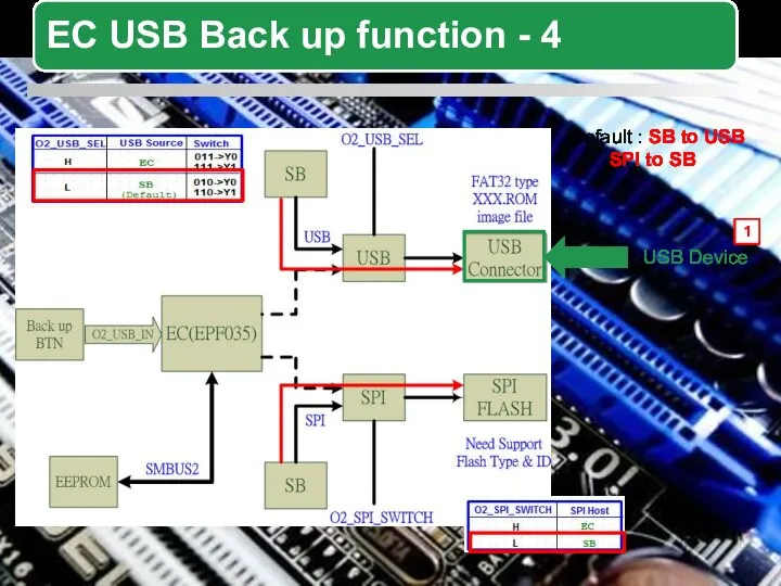
- 51. USB Device Default : SB to USB SPI to SB 1
- 52. USB Device At S5 status, press Backup button more than 3 sec to start back function.
- 53. USB Device 2 1 3 3 2
- 54. USB Device Confirm ROMID & MODELID and others information are normal 1 3 3 2 4
- 55. 1 3 3 2 4 5 5
- 60. When System BIOS update EC Firmware EC Broken status: EC flash is corrupted The data in
- 61. Power & Reset & XTAL: 24 MHz Crystal
- 62. O2_OP_mode: This PIN is used for RD & factory to update EC firmware or flash programming.
- 63. O2_PWM0~5:
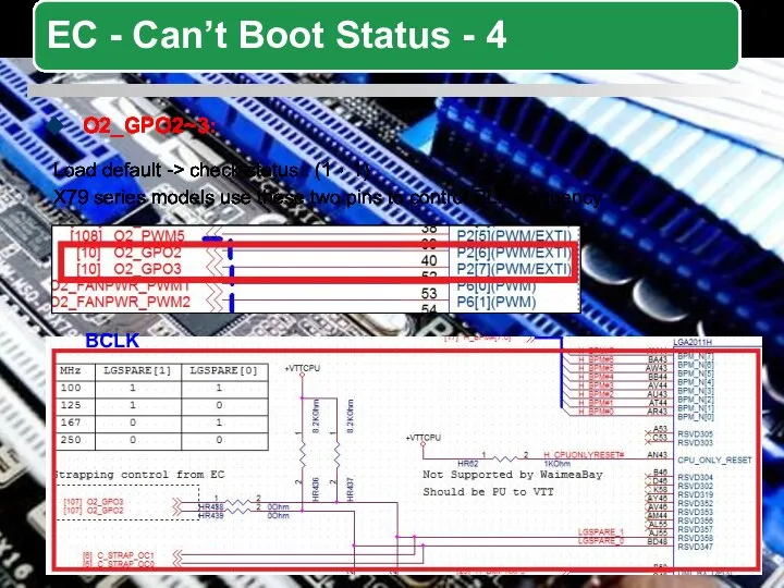
- 64. O2_GPO2~3: Load default -> check status : (1,1) X79 series models use these two pins to
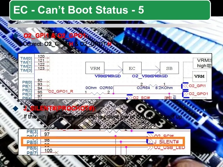
- 65. O2_GPI1 & O2_GPO1: Correct: O2_GPI1:H & O2_GPO1:H J_SILENT#(PROCHOT#): If this pin of X79 series model is
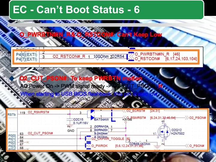
- 66. O_PWRBTN#IN_R& O_RSTCON#: Can’t Keep Low O2_CUT_PSON#: To keep PWRBTN motion AC Power On -> PWM signal
- 67. SMBUS & O2_SMB_SWITCH: Hang”0d0c” : EC check internal register setting of each DIGI+ Power Control.
- 68. Intel X79 Platform Structure P9X79 Series Architecture New Feature Difference With P8 Series Clock Distribution Power
- 69. 33MHz LPC Interface PECI Platform Environment Control Interface SMBus H/W Monitor PORT 80 Deep S5 KBMS
- 71. ASP1000 and ASP1101 are all DIGI power controller, all BIOS setting function can transmit signals through
- 72. Vcc=3.3V Vinsen = 0.86V VRHot = Vcc EN=3.3V The Sequence: VCC->Vinsen->VRHot->EN Others Signals: VSEN (FB+) RRES
- 73. Vcc=3.3V Vinsen = 0.86V VRHot = Vcc EN=3.3V The Sequence: VCC->Vinsen->VRHot->EN ASP1101 7.5 K Ohm
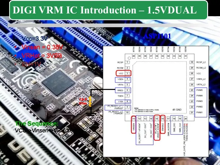
- 74. Vcc=3.3V Vinsen = 0.38V VRHot = 3VSB EN=1V The Sequence: VCC->Vinsen->VRHot->EN 7.5 K Ohm ASP1101
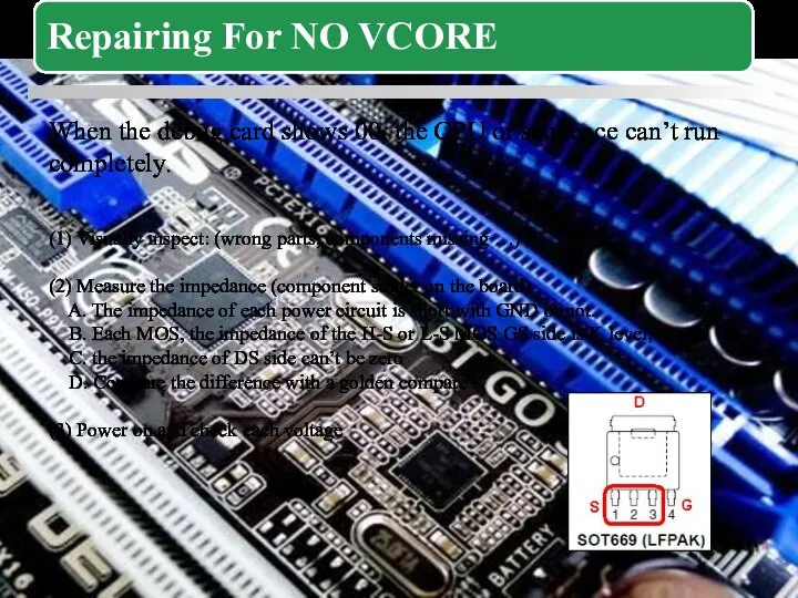
- 75. When the debug card shows 00, the CPU or sequence can’t run completely. (1) Visually inspect:
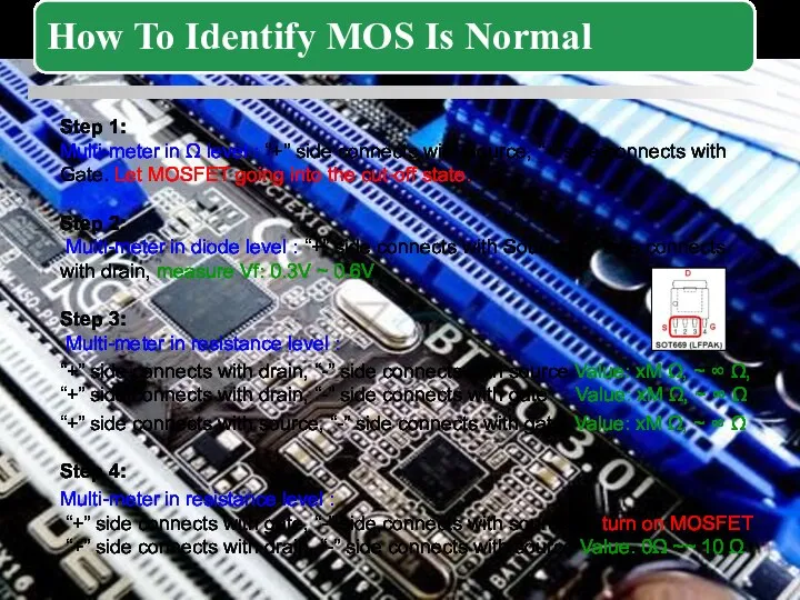
- 76. Step 1: Multi-meter in Ω level : “+” side connects with Source, “-” side connects with
- 77. Intel X79 Platform Structure P9X79 Series Architecture New Feature Difference With P8 Series Clock Distribution Power
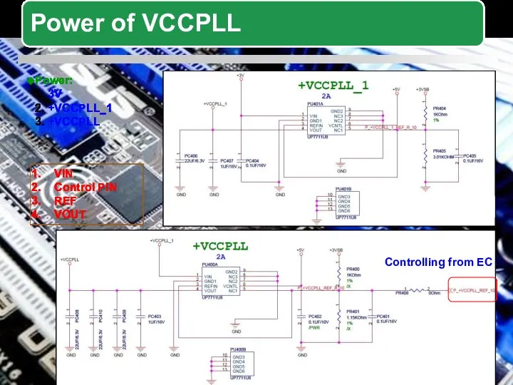
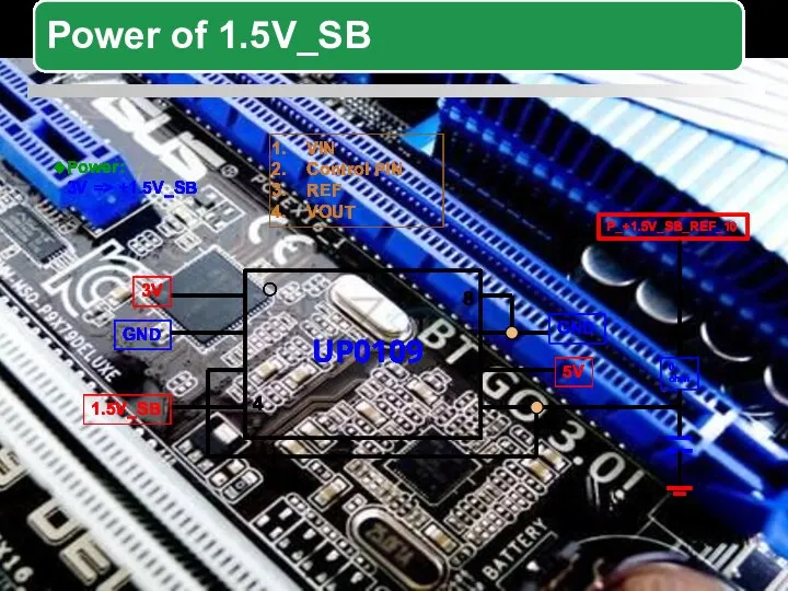
- 78. Controlling from EC VIN Control PIN REF VOUT Power: 1. 3V 2. +VCCPLL_1 3. +VCCPLL
- 79. VIN Control PIN REF VOUT UP0109 GND GND 3V 0 ohm 5V P_+1.5V_SB_REF_10 4 8 1.5V_SB
- 80. +d
- 81. SIO PR217 P_+VTTCPU_FB_R1_10 O_+VTTCPU_OV# Power: 12V=>+VTTCPU
- 82. 5V
- 83. 0 SIO PR527 P_+1.1V_SB_FB_R1_10 O_+1.1V_SB_OV#
- 84. Intel X79 Platform Structure P9X79 Series Architecture New Feature Difference With P8 Series Clock Distribution Power
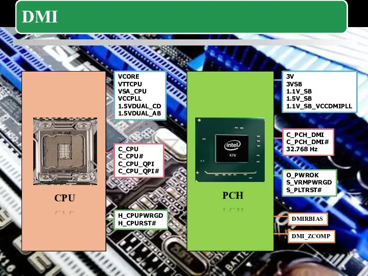
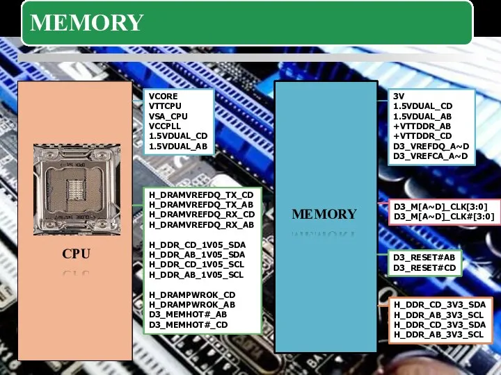
- 85. VCORE VTTCPU VSA_CPU VCCPLL 1.5VDUAL_CD 1.5VDUAL_AB C_CPU C_CPU# C_CPU_QPI C_CPU_QPI# H_CPUPWRGD H_CPURST# 3V 3VSB 1.1V_SB 1.5V_SB
- 86. H_DMI_TXP[3:0] H_DMI_TXN[3:0] H_DMI_RXP[3:0] H_DMI_RXN[3:0]
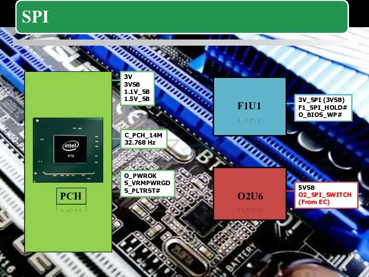
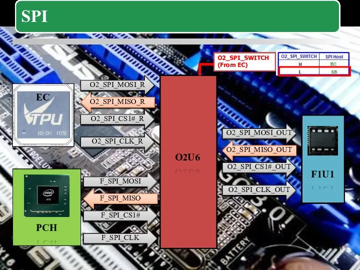
- 87. 3V 3VSB 1.1V_SB 1.5V_SB C_PCH_14M 32.768 Hz O_PWROK S_VRMPWRGD S_PLTRST# 3V_SPI (3VSB) F1_SPI_HOLD# O_BIOS_WP# 5VSB O2_SPI_SWITCH
- 88. O2_SPI_SWITCH (From EC)
- 89. VCORE VTTCPU VSA_CPU VCCPLL 1.5VDUAL_CD 1.5VDUAL_AB H_DRAMVREFDQ_TX_CD H_DRAMVREFDQ_TX_AB H_DRAMVREFDQ_RX_CD H_DRAMVREFDQ_RX_AB H_DDR_CD_1V05_SDA H_DDR_AB_1V05_SDA H_DDR_CD_1V05_SCL H_DDR_AB_1V05_SCL H_DRAMPWROK_CD H_DRAMPWROK_AB
- 90. D3_DQ_A[64:0] D3_DQS_A[7:0] D3_DQS_A#[3:0] A~D A~D
- 91. 3V 3VSB 1.1V_SB 1.5V_SB C_PCH_14M C_PCI_PCH 32.768 Hz O_PWROK S_VRMPWRGD S_PLTRST# SIO 3V 3VSB_ATX VTTCPU C_48M_SIO
- 92. F_SERIRQ# F_LAD[3:0]
- 94. Скачать презентацию
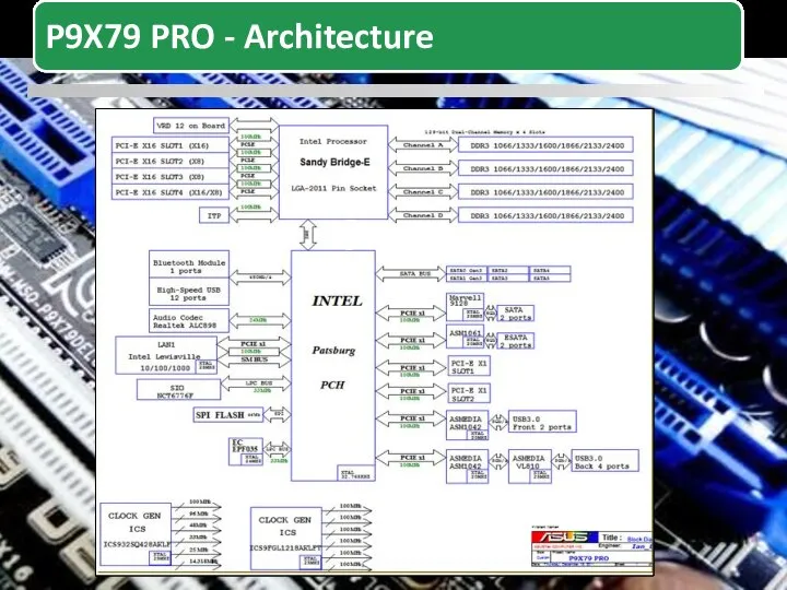
Intel X79 Platform Structure
P9X79 Series Architecture
New Feature
Difference With P8 Series
Clock
Intel X79 Platform Structure
P9X79 Series Architecture
New Feature
Difference With P8 Series
Clock

Intel X79 Platform Structure
P9X79 Series Architecture
New Feature
Difference With P8 Series
Clock
Intel X79 Platform Structure
P9X79 Series Architecture
New Feature
Difference With P8 Series
Clock
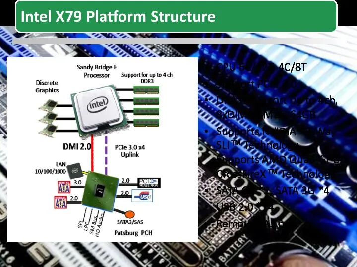
CPU 6C/12T, 4C/8T
Support PCIe 3.0
DRAM support up to 4ch, 8xDIMM, Max.
CPU 6C/12T, 4C/8T
Support PCIe 3.0
DRAM support up to 4ch, 8xDIMM, Max.
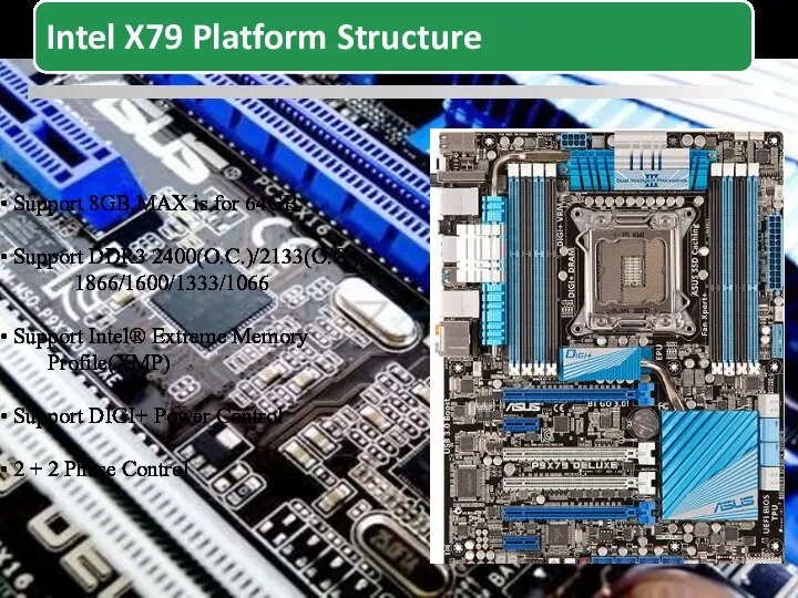
Support 8GB,MAX is for 64GB
Support DDR3 2400(O.C.)/2133(O.C.)
1866/1600/1333/1066
Support Intel®
Support 8GB,MAX is for 64GB
Support DDR3 2400(O.C.)/2133(O.C.)
1866/1600/1333/1066
Support Intel®
Intel X79 Platform Structure
P9X79 Series Architecture
New Feature
Difference With P8 Series
Clock
Intel X79 Platform Structure
P9X79 Series Architecture
New Feature
Difference With P8 Series
Clock

Intel X79 Platform Structure
P9X79 Series Architecture
New Feature
Difference With P8 Series
Clock
Intel X79 Platform Structure
P9X79 Series Architecture
New Feature
Difference With P8 Series
Clock
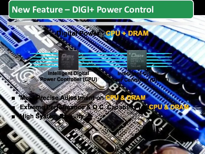
DIGI+ Power Control (2/6)
Most Precise Adjustment on CPU & DRAM
Extreme Performance
DIGI+ Power Control (2/6)
Most Precise Adjustment on CPU & DRAM
Extreme Performance
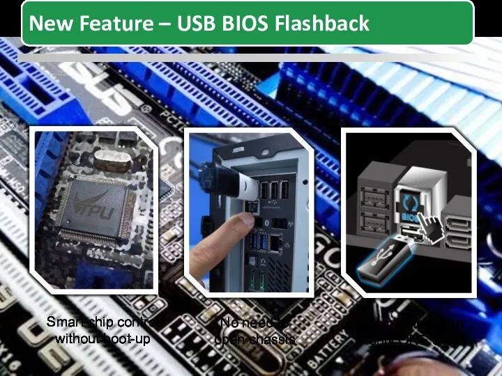
Smart chip control
without boot-up
No need to
open chassis
Complete within
only
Smart chip control
without boot-up
No need to
open chassis
Complete within
only

Intel X79 Platform Structure
P9X79 Series Architecture
New Feature
Difference With P8 Series
Clock
Intel X79 Platform Structure
P9X79 Series Architecture
New Feature
Difference With P8 Series
Clock
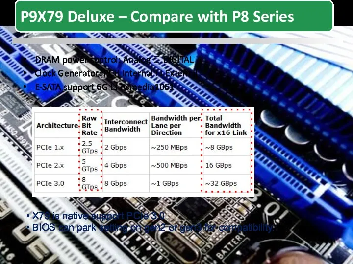
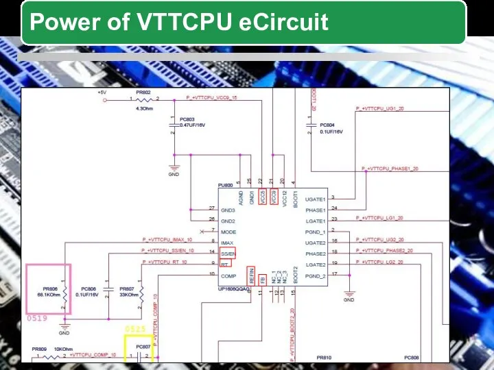
DRAM power control: Analog ? DIGITAL
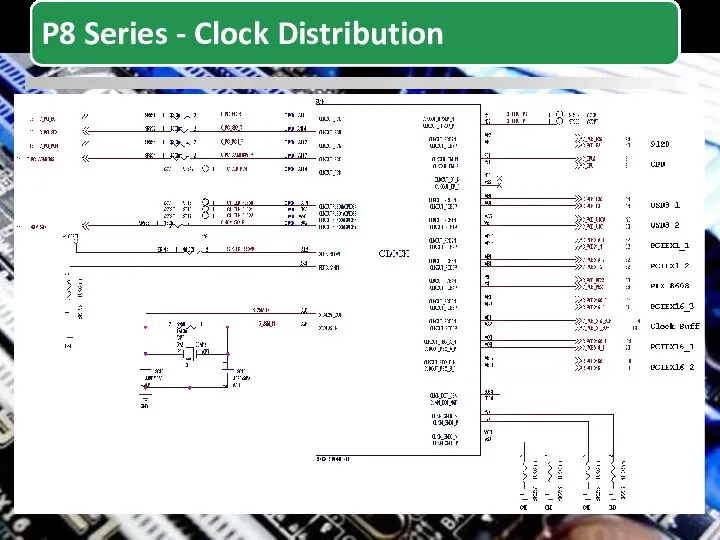
Clock Generator: PCH Internal ? External
DRAM power control: Analog ? DIGITAL
Clock Generator: PCH Internal ? External
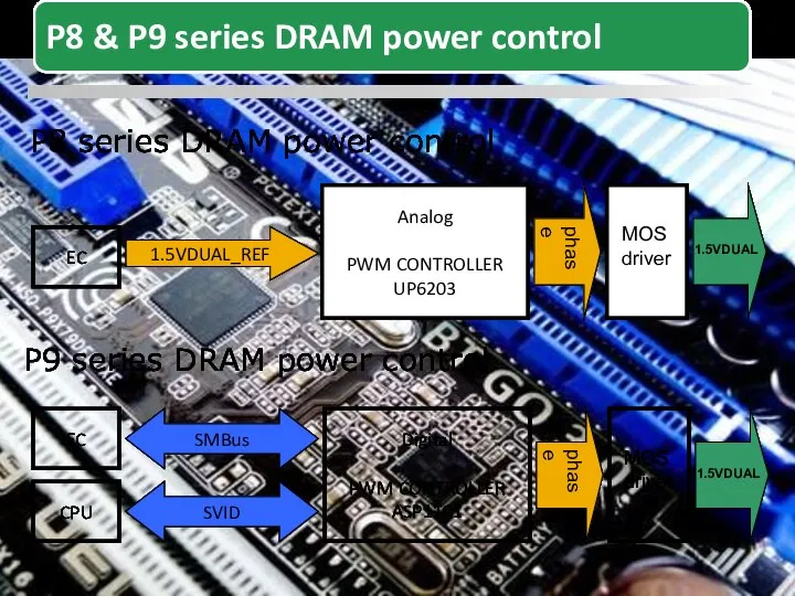
Analog
PWM CONTROLLER
UP6203
1.5VDUAL_REF
EC
phase
MOS
driver
1.5VDUAL
Digital
PWM CONTROLLER
ASP1101
EC
phase
MOS
driver
1.5VDUAL
CPU
SMBus
SVID
P9 series DRAM power control
P8 series DRAM
Analog
PWM CONTROLLER
UP6203
1.5VDUAL_REF
EC
phase
MOS
driver
1.5VDUAL
Digital
PWM CONTROLLER
ASP1101
EC
phase
MOS
driver
1.5VDUAL
CPU
SMBus
SVID
P9 series DRAM power control
P8 series DRAM

Intel X79 Platform Structure
P9X79 Series Architecture
New Feature
Difference With P8 Series
Clock
Intel X79 Platform Structure
P9X79 Series Architecture
New Feature
Difference With P8 Series
Clock
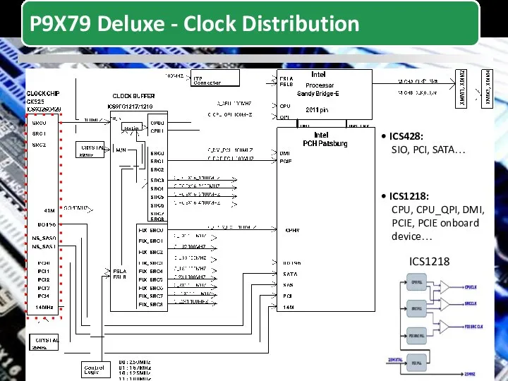
ICS428:
SIO, PCI, SATA…
ICS1218:
CPU, CPU_QPI,
ICS428:
SIO, PCI, SATA…
ICS1218:
CPU, CPU_QPI,
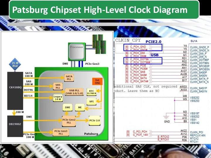
PCIE2.0
USB
PCIE2.0
USB
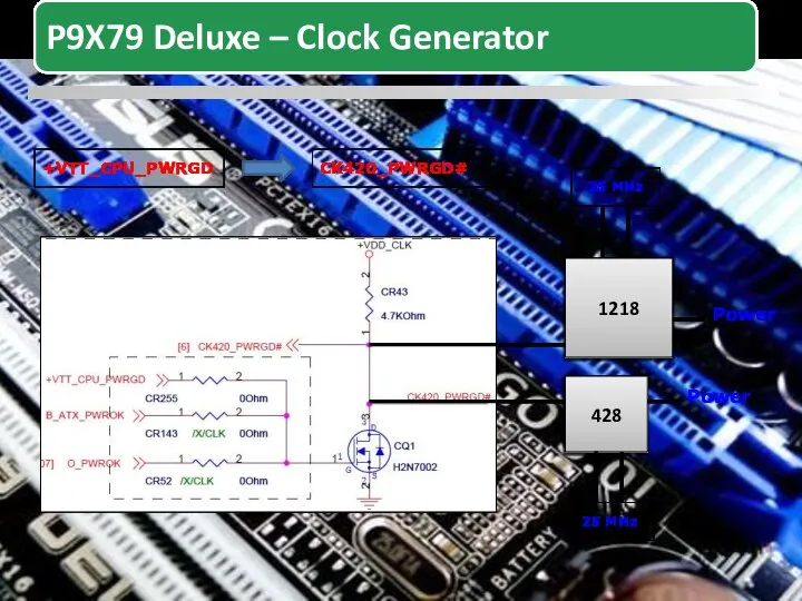
1218
428
+VTT_CPU_PWRGD
CK420_PWRGD#
25 MHz
25 MHz
Power
Power
1218
428
+VTT_CPU_PWRGD
CK420_PWRGD#
25 MHz
25 MHz
Power
Power
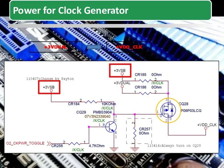
+3VDUAL
+VDD_CLK
+3VDUAL
+VDD_CLK
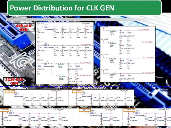
428 CLK GEN
1218 CLK GEN
428 CLK GEN
1218 CLK GEN

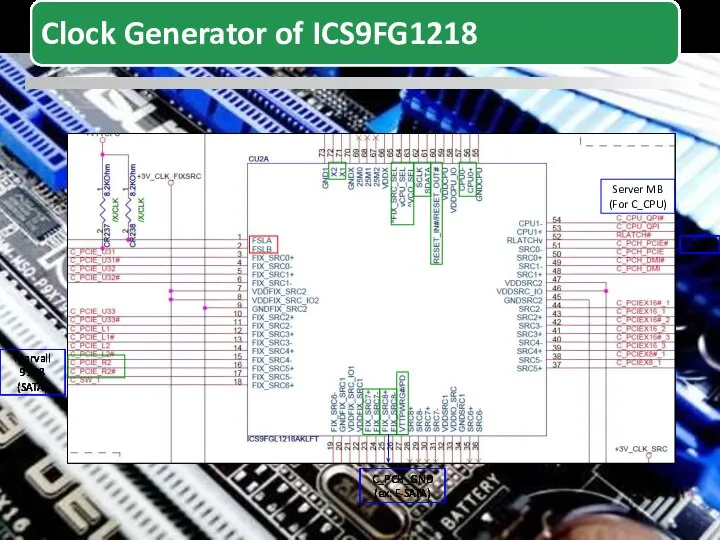
Server MB
(For C_CPU)
SAS
Marvall 9128
(SATA)
C_PCH_GND
(ex: E-SATA)
Server MB
(For C_CPU)
SAS
Marvall 9128
(SATA)
C_PCH_GND
(ex: E-SATA)

Intel X79 Platform Structure
P9X79 Series Architecture
New Feature
Difference With P8 Series
Clock
Intel X79 Platform Structure
P9X79 Series Architecture
New Feature
Difference With P8 Series
Clock


Intel X79 Platform Structure
P9X79 Series Architecture
New Feature
Difference With P8 Series
Clock
Intel X79 Platform Structure
P9X79 Series Architecture
New Feature
Difference With P8 Series
Clock
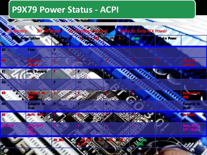
G3: Battery S0: All Power S3: Standby and Dual Deep S5: Only ATX Power
G3: Battery S0: All Power S3: Standby and Dual Deep S5: Only ATX Power
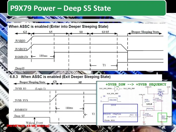
(PWRBTN#IN, KB MS Wakeup)
(PWRBTN#IN, KB MS Wakeup)

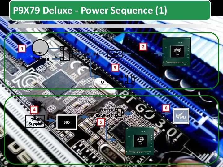
SIO
3V_ATX
+BAT_3V
SR88
S_SRTCRST
O2_ECRST#
Power Supply
O_RSMRST#
O2_ECRST#
O_RSMRST#
O2_RSMRST#
1
2
3
4
5
6
SIO
3V_ATX
+BAT_3V
SR88
S_SRTCRST
O2_ECRST#
Power Supply
O_RSMRST#
O2_ECRST#
O_RSMRST#
O2_RSMRST#
1
2
3
4
5
6
O2_ECRST#
O2_RSMRST#
P_+VCCPLL_REF +1.8V level (0.03V in S5)
P_+VTTCPU_REF +1.05V level (0.8V in S5)
P_+1.1V_SB_REF +1.1V level
P_+VTTDDR_AB_REF_10 +0.75V
O2_ECRST#
O2_RSMRST#
P_+VCCPLL_REF +1.8V level (0.03V in S5)
P_+VTTCPU_REF +1.05V level (0.8V in S5)
P_+1.1V_SB_REF +1.1V level
P_+VTTDDR_AB_REF_10 +0.75V
SIO
Power Button
O_PWRBTN#IN
O_PWRBTN#
SIO
SLP_S3#
SLP_S4#
O_PSON#
O2_CUT_PSON#
O2_PSON#
+3V level
+3V level
+3V level
+5V level
Power Supply
O2_PSON#
3V, 5V, 12V
Power Supply
B_ATX_PWROK
SIO
+3V level
+5V
SIO
Power Button
O_PWRBTN#IN
O_PWRBTN#
SIO
SLP_S3#
SLP_S4#
O_PSON#
O2_CUT_PSON#
O2_PSON#
+3V level
+3V level
+3V level
+5V level
Power Supply
O2_PSON#
3V, 5V, 12V
Power Supply
B_ATX_PWROK
SIO
+3V level
+5V
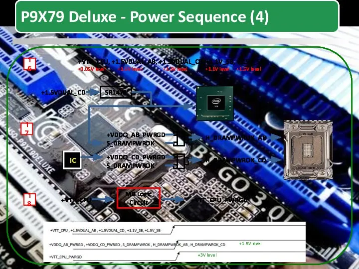
+VTT_CPU, +1.5VDUAL_AB, +1.5VDUAL_CD, +1.1V_SB, +1.5V_SB
+1.05V level
+1.5V level
+1.5V level
+1.1V level
+1.5V level
16
+VDDQ_AB_PWRGD
S_DRAMPWROK
+VDDQ_CD_PWRGD
S_DRAMPWROK
H_DRAMPWROK_AB
H_DRAMPWROK_CD
17
IC
SR1478
+1.5VDUAL_CD
+VTT_CPU
18
MB
+VTT_CPU, +1.5VDUAL_AB, +1.5VDUAL_CD, +1.1V_SB, +1.5V_SB
+1.05V level
+1.5V level
+1.5V level
+1.1V level
+1.5V level
16
+VDDQ_AB_PWRGD
S_DRAMPWROK
+VDDQ_CD_PWRGD
S_DRAMPWROK
H_DRAMPWROK_AB
H_DRAMPWROK_CD
17
IC
SR1478
+1.5VDUAL_CD
+VTT_CPU
18
MB
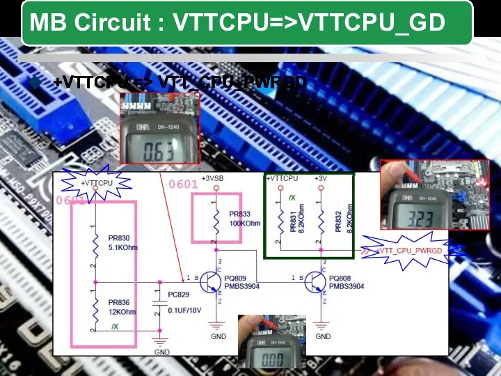
+VTTCPU => VTT_CPU_PWRGD
+VTTCPU => VTT_CPU_PWRGD
19
+VTT_CPU_PWRGD
VCORE
IC
VCCSA
IC
SR151
SR1003
P_VCORE_EN_10
P_VCCSA_EN_10
SR255
Clock Gen
MB Logic Circuit
20
21
VCORE
IC
VCCSA
IC
P_VCORE_EN_10
P_VCCSA_EN_10
+VCORE
+VCCSA
(Around +1V)
19
+VTT_CPU_PWRGD
VCORE
IC
VCCSA
IC
SR151
SR1003
P_VCORE_EN_10
P_VCCSA_EN_10
SR255
Clock Gen
MB Logic Circuit
20
21
VCORE
IC
VCCSA
IC
P_VCORE_EN_10
P_VCCSA_EN_10
+VCORE
+VCCSA
(Around +1V)
VCORE
IC
P_VCORE_VRDY_6
22
O2_GPI1
MB Logic Circuit
O2R64
S_VRMPWRGD
EC
O2_GPO1
SR535
O2_GPO1
+VSA_CPU_PWRGD
VCORE
IC
MB Logic Circuit
P_+VCCPLL_REF_R_10
23
P_+VCCPLL_REF_R_10
VCCPLL
IC
+VCCPLL
+1.8V level
VCORE
IC
P_VCORE_VRDY_6
22
O2_GPI1
MB Logic Circuit
O2R64
S_VRMPWRGD
EC
O2_GPO1
SR535
O2_GPO1
+VSA_CPU_PWRGD
VCORE
IC
MB Logic Circuit
P_+VCCPLL_REF_R_10
23
P_+VCCPLL_REF_R_10
VCCPLL
IC
+VCCPLL
+1.8V level
X
1
2
3
3
EC
5
4
5
6
X
1
2
3
3
EC
5
4
5
6
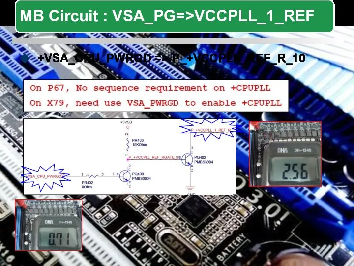
+VSA_CPU_PWRGD => P_+VCCPLL_REF_R_10
+VSA_CPU_PWRGD => P_+VCCPLL_REF_R_10
24
SIO
O_PWROK_SIO
EC
SR1478
O_PWROK
H_CPUPWRGD
H_SID_CLK
H_SID_DATA
H_SID_ALERT#
VCORE
IC
25
+3V level
+1.05V level
+1.05V level
24
SIO
O_PWROK_SIO
EC
SR1478
O_PWROK
H_CPUPWRGD
H_SID_CLK
H_SID_DATA
H_SID_ALERT#
VCORE
IC
25
+3V level
+1.05V level
+1.05V level
![S_VRMPWRGD 26 S_PLTRST# SIO LAN Other Devices 27 SIO O_PCIRST#_PCIEX16_* [1:3]](/_ipx/f_webp&q_80&fit_contain&s_1440x1080/imagesDir/jpg/1462586/slide-42.jpg)
S_VRMPWRGD
26
S_PLTRST#
SIO
LAN
Other Devices
27
SIO
O_PCIRST#_PCIEX16_* [1:3]
MB PCIE
S_PLTRST#
28
H_CPURST#
+3V level
+3V level
+1.05V level
S_VRMPWRGD
26
S_PLTRST#
SIO
LAN
Other Devices
27
SIO
O_PCIRST#_PCIEX16_* [1:3]
MB PCIE
S_PLTRST#
28
H_CPURST#
+3V level
+3V level
+1.05V level

Intel X79 Platform Structure
P9X79 Series Architecture
New Feature
Difference With P8 Series
Clock
Intel X79 Platform Structure
P9X79 Series Architecture
New Feature
Difference With P8 Series
Clock
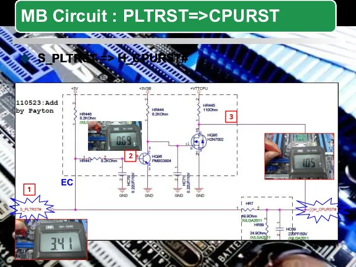
S_PLTRST => H_CPURST#
1
EC
2
3
S_PLTRST => H_CPURST#
1
EC
2
3
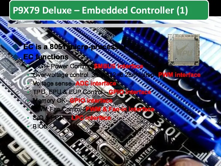
EC is a 8051 micro-processor
EC functions
DIGI+ Power Control--SMBUS interface
Over-voltage control,
EC functions
DIGI+ Power Control--SMBUS interface
Over-voltage control,

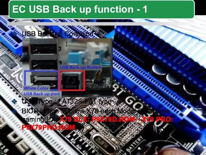
USB Back up Condition
USB Type : FAT32、FAT type
BIOS Image : Follow
USB Back up Condition
USB Type : FAT32、FAT type
BIOS Image : Follow
According these signals connecting to EC, EC can realize present system
According these signals connecting to EC, EC can realize present system

USB Device
Default : SB to USB
SPI to SB
1
USB Device
Default : SB to USB
SPI to SB
1

USB Device
At S5 status, press Backup button more than 3 sec
USB Device
At S5 status, press Backup button more than 3 sec
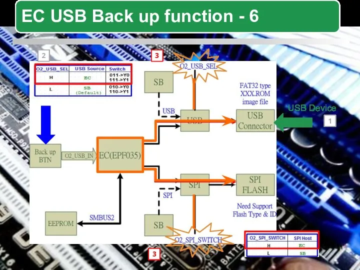
USB Device
2
1
3
3
2
USB Device
2
1
3
3
2
USB Device
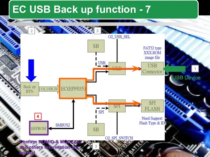
Confirm ROMID & MODELID and others information are normal
1
3
3
2
4
USB Device
Confirm ROMID & MODELID and others information are normal
1
3
3
2
4
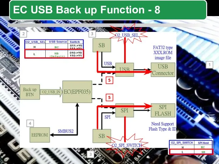
1
3
3
2
4
5
5
1
3
3
2
4
5
5


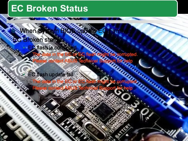
When System BIOS update EC Firmware
EC Broken status:
EC flash is corrupted
When System BIOS update EC Firmware
EC Broken status:
EC flash is corrupted
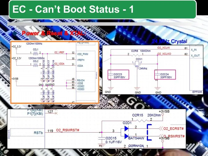
Power & Reset & XTAL:
24 MHz Crystal
Power & Reset & XTAL:
24 MHz Crystal
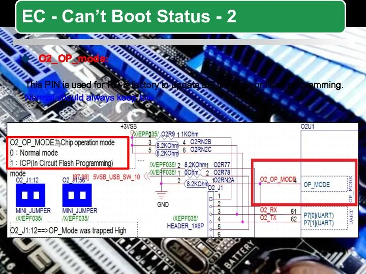
O2_OP_mode:
This PIN is used for RD & factory to update EC
O2_OP_mode:
This PIN is used for RD & factory to update EC
O2_PWM0~5:
O2_PWM0~5:
O2_GPO2~3:
Load default -> check status : (1,1)
X79 series models use these
O2_GPO2~3:
Load default -> check status : (1,1)
X79 series models use these
O2_GPI1 & O2_GPO1:
Correct: O2_GPI1:H & O2_GPO1:H
J_SILENT#(PROCHOT#):
If this pin of
O2_GPI1 & O2_GPO1:
Correct: O2_GPI1:H & O2_GPO1:H
J_SILENT#(PROCHOT#):
If this pin of
O_PWRBTN#IN_R& O_RSTCON#: Can’t Keep Low
O2_CUT_PSON#: To keep PWRBTN motion
AC Power
O_PWRBTN#IN_R& O_RSTCON#: Can’t Keep Low
O2_CUT_PSON#: To keep PWRBTN motion
AC Power
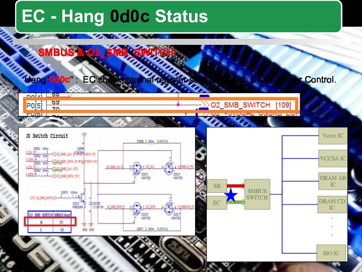
SMBUS & O2_SMB_SWITCH:
Hang”0d0c” : EC check internal register setting of
SMBUS & O2_SMB_SWITCH:
Hang”0d0c” : EC check internal register setting of

Intel X79 Platform Structure
P9X79 Series Architecture
New Feature
Difference With P8 Series
Clock
Intel X79 Platform Structure
P9X79 Series Architecture
New Feature
Difference With P8 Series
Clock
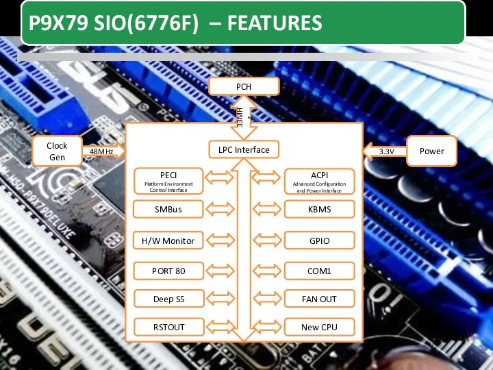
33MHz
LPC Interface
PECI
Platform Environment Control Interface
SMBus
H/W Monitor
PORT 80
Deep S5
KBMS
ACPI
Advanced Configuration and Power
33MHz
LPC Interface
PECI
Platform Environment Control Interface
SMBus
H/W Monitor
PORT 80
Deep S5
KBMS
ACPI
Advanced Configuration and Power


ASP1000 and ASP1101 are all DIGI power controller, all BIOS setting
ASP1000 and ASP1101 are all DIGI power controller, all BIOS setting
Vcc=3.3V
Vinsen = 0.86V
VRHot = Vcc
EN=3.3V
The Sequence:
VCC->Vinsen->VRHot->EN
Others Signals:
VSEN (FB+)
RRES
V18A
VR_READY
PIN17~19
SMBus
PWM signal
7.5 K Ohm
ASP1000
Vcc=3.3V
Vinsen = 0.86V
VRHot = Vcc
EN=3.3V
The Sequence:
VCC->Vinsen->VRHot->EN
Others Signals:
VSEN (FB+)
RRES
V18A
VR_READY
PIN17~19
SMBus
PWM signal
7.5 K Ohm
ASP1000
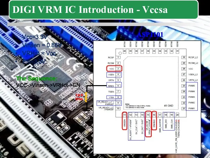
Vcc=3.3V
Vinsen = 0.86V
VRHot = Vcc
EN=3.3V
The Sequence:
VCC->Vinsen->VRHot->EN
ASP1101
7.5 K Ohm
Vcc=3.3V
Vinsen = 0.86V
VRHot = Vcc
EN=3.3V
The Sequence:
VCC->Vinsen->VRHot->EN
ASP1101
7.5 K Ohm
Vcc=3.3V
Vinsen = 0.38V
VRHot = 3VSB
EN=1V
The Sequence:
VCC->Vinsen->VRHot->EN
7.5 K Ohm
ASP1101
Vcc=3.3V
Vinsen = 0.38V
VRHot = 3VSB
EN=1V
The Sequence:
VCC->Vinsen->VRHot->EN
7.5 K Ohm
ASP1101
When the debug card shows 00, the CPU or sequence can’t
When the debug card shows 00, the CPU or sequence can’t
Step 1:
Multi-meter in Ω level : “+” side connects with Source,
Step 1: Multi-meter in Ω level : “+” side connects with Source,

Intel X79 Platform Structure
P9X79 Series Architecture
New Feature
Difference With P8 Series
Clock
Intel X79 Platform Structure
P9X79 Series Architecture
New Feature
Difference With P8 Series
Clock
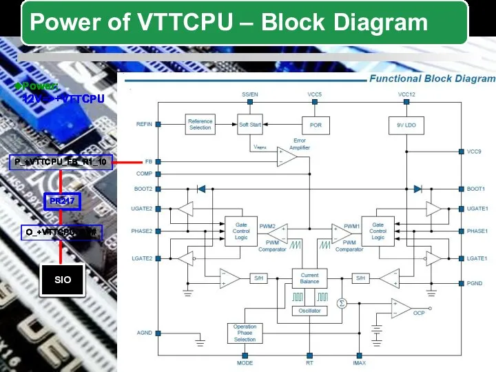
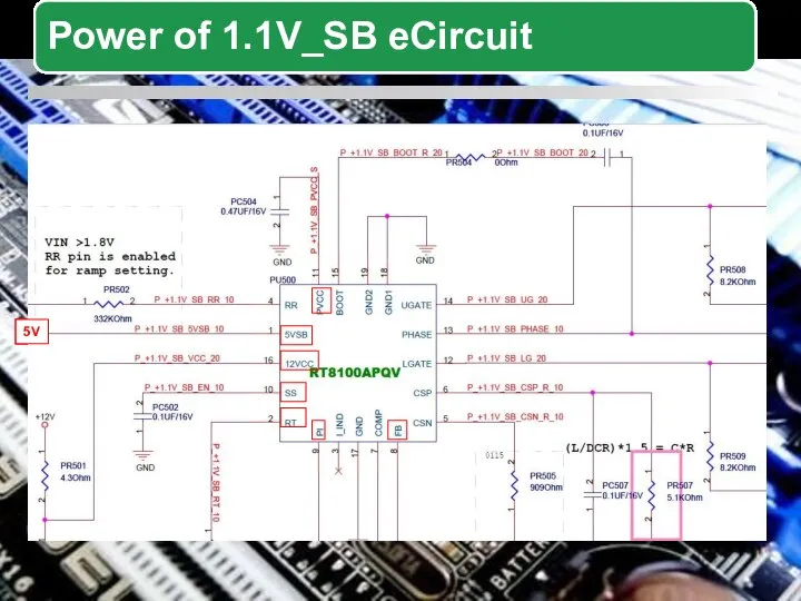
Controlling from EC
VIN
Control PIN
REF
VOUT
Power:
1. 3V
2. +VCCPLL_1
3. +VCCPLL
Controlling from EC
VIN
Control PIN
REF
VOUT
Power:
1. 3V
2. +VCCPLL_1
3. +VCCPLL
VIN
Control PIN
REF
VOUT
UP0109
GND
GND
3V
0
ohm
5V
P_+1.5V_SB_REF_10
4
8
1.5V_SB
Power:
3V => +1.5V_SB
VIN
Control PIN
REF
VOUT
UP0109
GND
GND
3V
0
ohm
5V
P_+1.5V_SB_REF_10
4
8
1.5V_SB
Power:
3V => +1.5V_SB
+d
+d
SIO
PR217
P_+VTTCPU_FB_R1_10
O_+VTTCPU_OV#
Power:
12V=>+VTTCPU
SIO
PR217
P_+VTTCPU_FB_R1_10
O_+VTTCPU_OV#
Power:
12V=>+VTTCPU
5V
5V
0
SIO
PR527
P_+1.1V_SB_FB_R1_10
O_+1.1V_SB_OV#
0
SIO
PR527
P_+1.1V_SB_FB_R1_10
O_+1.1V_SB_OV#

Intel X79 Platform Structure
P9X79 Series Architecture
New Feature
Difference With P8 Series
Clock
Intel X79 Platform Structure
P9X79 Series Architecture
New Feature
Difference With P8 Series
Clock
VCORE
VTTCPU
VSA_CPU
VCCPLL
1.5VDUAL_CD
1.5VDUAL_AB
C_CPU
C_CPU#
C_CPU_QPI
C_CPU_QPI#
H_CPUPWRGD
H_CPURST#
3V
3VSB
1.1V_SB
1.5V_SB
1.1V_SB_VCCDMIPLL
C_PCH_DMI
C_PCH_DMI#
32.768 Hz
O_PWROK
S_VRMPWRGD
S_PLTRST#
DMI_ZCOMP
DMIRBIAS
VCORE
VTTCPU
VSA_CPU
VCCPLL
1.5VDUAL_CD
1.5VDUAL_AB
C_CPU
C_CPU#
C_CPU_QPI
C_CPU_QPI#
H_CPUPWRGD
H_CPURST#
3V
3VSB
1.1V_SB
1.5V_SB
1.1V_SB_VCCDMIPLL
C_PCH_DMI
C_PCH_DMI#
32.768 Hz
O_PWROK
S_VRMPWRGD
S_PLTRST#
DMI_ZCOMP
DMIRBIAS
![H_DMI_TXP[3:0] H_DMI_TXN[3:0] H_DMI_RXP[3:0] H_DMI_RXN[3:0]](/_ipx/f_webp&q_80&fit_contain&s_1440x1080/imagesDir/jpg/1462586/slide-85.jpg)
H_DMI_TXP[3:0]
H_DMI_TXN[3:0]
H_DMI_RXP[3:0]
H_DMI_RXN[3:0]
H_DMI_TXP[3:0]
H_DMI_TXN[3:0]
H_DMI_RXP[3:0]
H_DMI_RXN[3:0]
3V
3VSB
1.1V_SB
1.5V_SB
C_PCH_14M
32.768 Hz
O_PWROK
S_VRMPWRGD
S_PLTRST#
3V_SPI (3VSB)
F1_SPI_HOLD#
O_BIOS_WP#
5VSB
O2_SPI_SWITCH
(From EC)
3V
3VSB
1.1V_SB
1.5V_SB
C_PCH_14M
32.768 Hz
O_PWROK
S_VRMPWRGD
S_PLTRST#
3V_SPI (3VSB)
F1_SPI_HOLD#
O_BIOS_WP#
5VSB
O2_SPI_SWITCH
(From EC)
O2_SPI_SWITCH
(From EC)
O2_SPI_SWITCH
(From EC)
VCORE
VTTCPU
VSA_CPU
VCCPLL
1.5VDUAL_CD
1.5VDUAL_AB
H_DRAMVREFDQ_TX_CD
H_DRAMVREFDQ_TX_AB
H_DRAMVREFDQ_RX_CD
H_DRAMVREFDQ_RX_AB
H_DDR_CD_1V05_SDA
H_DDR_AB_1V05_SDA
H_DDR_CD_1V05_SCL
H_DDR_AB_1V05_SCL
H_DRAMPWROK_CD
H_DRAMPWROK_AB
D3_MEMHOT#_AB
D3_MEMHOT#_CD
3V
1.5VDUAL_CD
1.5VDUAL_AB
+VTTDDR_AB
+VTTDDR_CD
D3_VREFDQ_A~D
D3_VREFCA_A~D
D3_M[A~D]_CLK[3:0]
D3_M[A~D]_CLK#[3:0]
D3_RESET#AB
D3_RESET#CD
H_DDR_CD_3V3_SDA
H_DDR_AB_3V3_SCL
H_DDR_CD_3V3_SDA
H_DDR_AB_3V3_SCL
![D3_DQ_A[64:0] D3_DQS_A[7:0] D3_DQS_A#[3:0] A~D A~D](/_ipx/f_webp&q_80&fit_contain&s_1440x1080/imagesDir/jpg/1462586/slide-89.jpg)
D3_DQ_A[64:0]
D3_DQS_A[7:0]
D3_DQS_A#[3:0]
A~D
A~D
D3_DQ_A[64:0]
D3_DQS_A[7:0]
D3_DQS_A#[3:0]
A~D
A~D
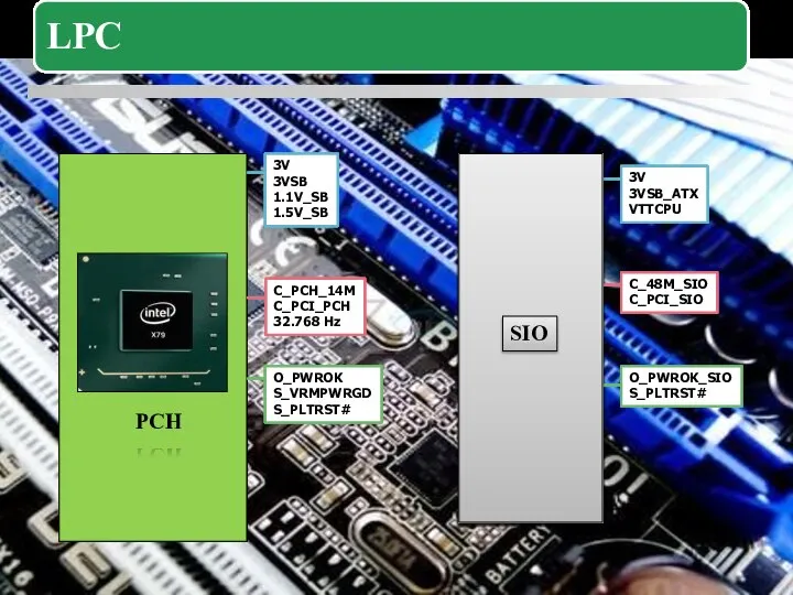
3V
3VSB
1.1V_SB
1.5V_SB
C_PCH_14M
C_PCI_PCH
32.768 Hz
O_PWROK
S_VRMPWRGD
S_PLTRST#
SIO
3V
3VSB_ATX
VTTCPU
C_48M_SIO
C_PCI_SIO
O_PWROK_SIO
S_PLTRST#
3V
3VSB
1.1V_SB
1.5V_SB
C_PCH_14M
C_PCI_PCH
32.768 Hz
O_PWROK
S_VRMPWRGD
S_PLTRST#
SIO
3V
3VSB_ATX
VTTCPU
C_48M_SIO
C_PCI_SIO
O_PWROK_SIO
S_PLTRST#
![F_SERIRQ# F_LAD[3:0]](/_ipx/f_webp&q_80&fit_contain&s_1440x1080/imagesDir/jpg/1462586/slide-91.jpg)
F_SERIRQ#
F_LAD[3:0]
F_SERIRQ#
F_LAD[3:0]
 Фокина Л. П. Викторина-раскраска ПРОФЕССИИ - презентация для начальной школы
 статистика трудовых ресурсов
  Презентация
 умножение и деление на 8 - презентация для начальной школы
 Презентация на тему "Химия жизни. Наследственные болезни, их профилактика и лечение" - скачать презентации по Медицине
 Мотивация и результативность спортивной деятельности
 Чайковский Петр Ильич
 Фокина Л. П. Игра СКАЗКА О ЗОЛОТОМ ПЕТУШКЕ - презентация для начальной школы
 Своя игра по сказкам К.И. Чуковского
  История формирования науки(античные времена)
 Национальность: осетины
 Meine mahlzeiten
 Виды тяжелого бетона
 СИФИЛИС « белая чума »
  Специальные налоговые режимы
 Презентация "Скульптура АНТИЧНОСТИ" - скачать презентации по МХК
 Фокина Л. П. Игра СКАЗКА О РЫБАКЕ И РЫБКЕ - презентация для начальной школы
 Презентация Международные стандарты социального обеспечения в Германии, в Нидерландах и в Италии
  Презентация по курсу «Основы информационных технологий» Руководитель: ст. преподаватель Воробьёв Михаил Алексеевич Выполнила:
  Кибернетическая модель управления
 Тоғызқұмалақ тарихы
 Если хочешь быть здоров, закаливайся - презентация для начальной школы
 2_5445196835364799410
 Презентация к урока 1-2
 Роман Юрьевич Катасонов - майор, погибший при освобождении заложников во время теракта в Беслане
 Тест по культуре Индии 8 класс автор учитель МХК Страхова Нина Павлиновна МОУ «СОШ №20 с УИОП» г.Ухта РК
 Моя Рикасиха
 Создание библиотек компонентов в пакете сапр altium designer