- Placement and routing guidelines for Power Electronics Devices

Содержание
- 2. Lecture plan Planning the layout. Single-board PCB layout. Placement of Layers for PE devices. Current loops
- 3. Current position: 1/7 Planning the layout. Single-board PCB layout. Placement of Layers for PE devices. Current
- 4. PCB design for PE devices. Why is it so important? Improper PCB design leads to: "unstable"
- 5. Planning the layout. Each PE device contains power part and control scheme. Power part - DC/DC,
- 6. Planning the layout. Do we need to separate power and control on to two different PCB’s?
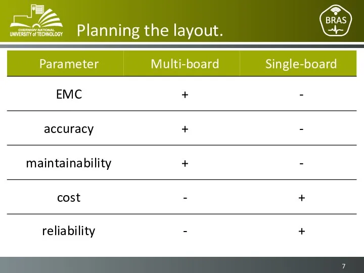
- 7. Planning the layout.
- 8. Current position: 2/7 Planning the layout. Single-board PCB layout. Placement of Layers for PE devices. Current
- 9. Single-board PCB layout. Power part location should be done at the first stage of PCB layout.
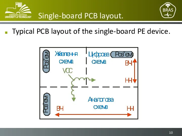
- 10. Single-board PCB layout. Typical PCB layout of the single-board PE device.
- 11. Single-board PCB layout. High speed components (both analog and digital) need to be placed as close
- 12. Current position: 3/7 Planning the layout. Single-board PCB layout. Placement of Layers for PE devices. Current
- 13. Stack of layers – 1, 2 or more? 1-layer PCB: Most sensitive to crosstalk and another
- 14. Stack of layers – 1, 2 or more? Multi-layer PCB: Better than 2-layer – more space
- 15. Stack of layers – 1, 2 or more? Conclusion: 1-layer PCBs – exceptional cases. 2-layer PCBs
- 16. Desirable stack of layers Typical stack of 4-layers PCB
- 17. Desirable stack of layers Typical stack of 6-layers PCB
- 18. Current position: 4/7 Planning the layout. Single-board PCB layout. Placement of Layers for PE devices. Current
- 19. Important features of power part Highest currents and voltages in the device What ever – mA
- 20. Buck Converter
- 21. Current loops ordered by EMI generation in power conv. 1. Power switch loop – maximum attention!
- 22. Boost converter
- 23. Transformer Isolated Flyback Converter
- 24. The first rule for PE devices PCB design. 1. The pulse loop circumference must be as
- 25. PCB layout for buck converter. Red – power switch loop, blue – rectifier loop. cross select
- 26. Red – rectifier loop, black – load loop. Output Rectifier Loop in Flyback Converter
- 27. Parallel C Filter Layout
- 28. Parallel C Filter Layout PCB layout between each capacitor and source in multi-component filter must be
- 29. Current position: 5/7 Planning the layout. Single-board PCB layout. Placement of Layers for PE devices. Current
- 30. Grounding in the PE devices. Types of ground in power convertor devices: Power ground with high
- 31. Grounding in buck converter Red – control ground, blue – power ground.
- 32. Control and power ground connection. Rules of thumb for grounding in PE devices: Feedback ground must
- 33. Grounding in flyback converter
- 34. Current position: 6/7 Planning the layout. Single-board PCB layout. Placement of Layers for PE devices. Current
- 35. Current sensor resistor PCB layout consideration The best characteristic provides 4-wire Kelvin sensing. Example of using
- 36. Current sensor resistor PCB layout consideration Sensing trace should be placed on opposite layer and connect
- 37. Land Patterns for SMD components in PE devices For minimization of ESL and ESR Pad configuration
- 38. Land Patterns for SMD components in PE devices Examples of Pad configuration:
- 39. Current position: 7/7 Planning the layout. Single-board PCB layout. Placement of Layers for PE devices. Current
- 40. Mixed-signal grounding Mixed-signal components: External DAC and ADC, MCU with DAC/ADC on board. Ground in mixed-signal
- 41. Mixed-signal grounding Mixed-signal components: External DAC and ADC, MCU with DAC/ADC on board. Ground in mixed-signal
- 42. Digital and Analog Ground Bed design: Digital (“dirty”) and analog (“clean”) ground are common – AGND
- 43. Digital and Analog Ground Good design: Digital and analog ground are separated.
- 44. Digital and Analog Ground Planes for ground in control circuits of power electronic devices should improve
- 45. Mixed-signal grounding – single PCB “Star” grounding in the control part of single-board PE device –
- 46. Mixed-signal grounding – single PCB “Star” grounding in the control part f single-board PE device –
- 47. Mixed-signal grounding – multi-board PCB Grounding techniques for single-board PE devices are not optimum for multi-board
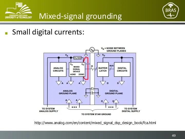
- 48. Mixed-signal grounding Small digital currents:
- 49. Mixed-signal grounding Small digital currents: http://www.analog.com/en/content/mixed_signal_dsp_design_book/fca.html
- 50. Mixed-signal grounding High digital currents: http://www.analog.com/en/content/mixed_signal_dsp_design_book/fca.html
- 51. Bypass Capacitors Noise on power line caused by switching digital components is shunted through the bypass
- 52. Bypass Capacitors Bypass capacitor should be connected to the power pins of the digital components as
- 54. Скачать презентацию

Lecture plan
Planning the layout.
Single-board PCB layout.
Placement of Layers for PE devices.
Current
Lecture plan
Planning the layout.
Single-board PCB layout.
Placement of Layers for PE devices.
Current

Current position: 1/7
Planning the layout.
Single-board PCB layout.
Placement of Layers for PE
Current position: 1/7
Planning the layout.
Single-board PCB layout.
Placement of Layers for PE

PCB design for PE devices. Why is it so important?
Improper PCB
PCB design for PE devices. Why is it so important?
Improper PCB

Planning the layout.
Each PE device contains power part and control scheme.
Power
Planning the layout.
Each PE device contains power part and control scheme.
Power

Planning the layout.
Do we need to separate power and control on
Planning the layout.
Do we need to separate power and control on
Planning the layout.
Planning the layout.

Current position: 2/7
Planning the layout.
Single-board PCB layout.
Placement of Layers for PE
Current position: 2/7
Planning the layout.
Single-board PCB layout.
Placement of Layers for PE

Single-board PCB layout.
Power part location should be done at the first
Single-board PCB layout.
Power part location should be done at the first
Single-board PCB layout.
Typical PCB layout of the single-board PE device.
Single-board PCB layout.
Typical PCB layout of the single-board PE device.

Single-board PCB layout.
High speed components (both analog and digital) need to
Single-board PCB layout.
High speed components (both analog and digital) need to

Current position: 3/7
Planning the layout.
Single-board PCB layout.
Placement of Layers for PE
Current position: 3/7
Planning the layout.
Single-board PCB layout.
Placement of Layers for PE

Stack of layers – 1, 2 or more?
1-layer PCB:
Most sensitive to
Stack of layers – 1, 2 or more?
1-layer PCB:
Most sensitive to
Stack of layers – 1, 2 or more?
Multi-layer PCB:
Better than 2-layer
Stack of layers – 1, 2 or more?
Multi-layer PCB:
Better than 2-layer

Stack of layers – 1, 2 or more?
Conclusion:
1-layer PCBs – exceptional
Stack of layers – 1, 2 or more?
Conclusion:
1-layer PCBs – exceptional

Desirable stack of layers
Typical stack of 4-layers PCB
Desirable stack of layers
Typical stack of 4-layers PCB

Desirable stack of layers
Typical stack of 6-layers PCB
Desirable stack of layers
Typical stack of 6-layers PCB

Current position: 4/7
Planning the layout.
Single-board PCB layout.
Placement of Layers for PE
Current position: 4/7
Planning the layout.
Single-board PCB layout.
Placement of Layers for PE

Important features of power part
Highest currents and voltages in the device
What
Important features of power part
Highest currents and voltages in the device
What

Buck Converter
Buck Converter

Current loops ordered by EMI generation in power conv.
1. Power switch
Current loops ordered by EMI generation in power conv.
1. Power switch

Boost converter
Boost converter

Transformer Isolated Flyback Converter
Transformer Isolated Flyback Converter

The first rule for PE devices PCB design.
1. The pulse loop
The first rule for PE devices PCB design.
1. The pulse loop

PCB layout for buck converter.
Red – power switch loop, blue –
PCB layout for buck converter.
Red – power switch loop, blue –

Red – rectifier loop, black – load loop.
Output Rectifier Loop
Red – rectifier loop, black – load loop.
Output Rectifier Loop

Parallel C Filter Layout
Parallel C Filter Layout

Parallel C Filter Layout
PCB layout between each capacitor and source in
Parallel C Filter Layout
PCB layout between each capacitor and source in

Current position: 5/7
Planning the layout.
Single-board PCB layout.
Placement of Layers for PE
Current position: 5/7
Planning the layout.
Single-board PCB layout.
Placement of Layers for PE

Grounding in the PE devices.
Types of ground in power convertor devices:
Power
Grounding in the PE devices.
Types of ground in power convertor devices:
Power

Grounding in buck converter
Red – control ground, blue – power ground.
Grounding in buck converter
Red – control ground, blue – power ground.

Control and power ground connection.
Rules of thumb for grounding in PE
Control and power ground connection.
Rules of thumb for grounding in PE

Grounding in flyback converter
Grounding in flyback converter

Current position: 6/7
Planning the layout.
Single-board PCB layout.
Placement of Layers for PE
Current position: 6/7
Planning the layout.
Single-board PCB layout.
Placement of Layers for PE

Current sensor resistor PCB layout consideration
The best characteristic provides 4-wire Kelvin
Current sensor resistor PCB layout consideration
The best characteristic provides 4-wire Kelvin

Current sensor resistor PCB layout consideration
Sensing trace should be placed on opposite
Current sensor resistor PCB layout consideration
Sensing trace should be placed on opposite
Land Patterns for SMD components in PE devices
For minimization of ESL
Land Patterns for SMD components in PE devices
For minimization of ESL

Land Patterns for SMD components in PE devices
Examples of Pad configuration:
Land Patterns for SMD components in PE devices
Examples of Pad configuration:

Current position: 7/7
Planning the layout.
Single-board PCB layout.
Placement of Layers for PE
Current position: 7/7
Planning the layout.
Single-board PCB layout.
Placement of Layers for PE

Mixed-signal grounding
Mixed-signal components:
External DAC and ADC, MCU with DAC/ADC on board.
Ground
Mixed-signal grounding
Mixed-signal components:
External DAC and ADC, MCU with DAC/ADC on board.
Ground

Mixed-signal grounding
Mixed-signal components:
External DAC and ADC, MCU with DAC/ADC on board.
Ground
Mixed-signal grounding
Mixed-signal components:
External DAC and ADC, MCU with DAC/ADC on board.
Ground

Digital and Analog Ground
Bed design:
Digital (“dirty”) and analog (“clean”) ground are
Digital and Analog Ground
Bed design:
Digital (“dirty”) and analog (“clean”) ground are

Digital and Analog Ground
Good design:
Digital and analog ground are separated.
Digital and Analog Ground
Good design:
Digital and analog ground are separated.

Digital and Analog Ground
Planes for ground in control circuits of power
Digital and Analog Ground
Planes for ground in control circuits of power

Mixed-signal grounding –
single PCB
“Star” grounding in the control part of
Mixed-signal grounding –
single PCB
“Star” grounding in the control part of

Mixed-signal grounding –
single PCB
“Star” grounding in the control part f
Mixed-signal grounding –
single PCB
“Star” grounding in the control part f

Mixed-signal grounding –
multi-board PCB
Grounding techniques for single-board PE devices are
Mixed-signal grounding –
multi-board PCB
Grounding techniques for single-board PE devices are

Mixed-signal grounding
Small digital currents:
Mixed-signal grounding
Small digital currents:
Mixed-signal grounding
Small digital currents:
http://www.analog.com/en/content/mixed_signal_dsp_design_book/fca.html
Mixed-signal grounding
Small digital currents:
http://www.analog.com/en/content/mixed_signal_dsp_design_book/fca.html

Mixed-signal grounding
High digital currents:
http://www.analog.com/en/content/mixed_signal_dsp_design_book/fca.html
Mixed-signal grounding
High digital currents:
http://www.analog.com/en/content/mixed_signal_dsp_design_book/fca.html

Bypass Capacitors
Noise on power line caused by switching digital components is
Bypass Capacitors
Noise on power line caused by switching digital components is

Bypass Capacitors
Bypass capacitor should be connected to the power pins of
Bypass Capacitors
Bypass capacitor should be connected to the power pins of
 Федеральный закон РФ о наркотических средствах и психотропных веществах
 Закономерности диффузии дыхательных газов
 Вспомогательное оборудование печатных машин
 Двухэтажный каттедж с мансардой в блокированной застройке
 Корпоративные производственные системы. Лекция 4
 Органическая химия – это наука, изучающая соединения углерода, или её ещё называют химией соединений углерода. Название «органиче
 Наше Отечество - презентация для начальной школы
 Основные разделы правовой статистики
 По математической сказке… МОУ «Сорская СОШ №3 с УИОП» Учитель: Канаева Татьяна Анатольевна
 Зацветёт, зазеленеет наш весёлый огород.
 Новый Титаник
 FK Barcelona
 Библейские притчи. Притча о добром самарянине
 Боевые искусства Древней Руси
 Структурные типы данных (Delphi / Pascal, глава 3)
 Рукводство по заполнению отчета по практике
 Леонардо Да Винчи: гениальная личность
 Как люди ныряют в воду
 Гражданское общество: понятие, подсистемы, функции. Подготовила: Мишина Дарья
 Гигиеническое стоматологическое обучение и воспитание детей в организованных коллективах Санитарное просвещение – составн
 Словообразование и словоизменение. Обобщение. Учитель начальных классов МАОУ «Лицей №62» г. Саратова Лукьянова Ольга Анатоль
 Phraseologie
 Туберкулез и сахарный диабет
 Волейбол
  Болонский процесс
 конференция отцов Гораздо легче стать отцом, чем остаться им В.Ключевский
 Презентация "А.С.Пушкин на портретах художников О.Кипренского и В.Тропинина" - скачать презентации по МХК
 Тестирование программного обеспечения. История и основные понятия