- Материалы и технологии изготовления нано- и микро-электромеханических систем НЭМС/МЭМС

Содержание
- 2. “It was the best of times, it was the worst of times, it was the age
- 3. Устройства памяти 35 Xe atoms
- 4. Оптическая система. Optical system. Photograph of a Fresnel microlens on an adjustable platform made of five
- 5. Photograph of the NovaSensor NPP-301, a premolded plastic, surface mount (SOIC-type) and absolute pressure sensor. (Courtesy
- 6. Photograph of a disposable blood pressure sensor for arterial-line measurement in intensive care units. The die
- 7. Преимущества Si как базового материала НЭМС Advantages of Si in NEMS/MEMS Дешевизна. Cheap. Высокое кристаллическое совершенство.
- 8. Формы и содинения кремния. Si forms and compounds. Crystalline silicon is a hard and brittle material
- 9. Физические свойства некоторых материалов НЭМС
- 10. Тонкие пленки металлов в НЭМС
- 11. Оптическое отражение от кремния и некоторых металлов Reflectivity of Si and some metals
- 12. Области применения различных материалов в НЭМС. Application areas of MEMS materials.
- 13. Базовый цикл создания НЭМС. Base cycle of NEMS formation.
- 14. Маркировка пластин полупроводников. Marking of wafers. (a) Illustration showing the primary and secondary flats of {100}
- 15. Эпитаксия кремния – молекулярно-лучевая или газофазная Epitaxy of Si – MBE and VPE Массовое промышленное производство
- 16. CVD Химическое осаждение из газовой фазы. Chemical vapor deposition Temperature > 300 °C. Growth rate from
- 17. Термическое окисление. Thermal oxidation Атмосфера кислорода, oxygen flux, 850-1150 °С. Аморфный SiO2, толщина зависит от температуры,
- 18. Распыление Sputtering Бомбардировка ионами, возможно в присутствии внешних полей: СВЧ, магнетронное, и др. Bombardment of target
- 19. Испарение Evaporation Термическое, лазерное, электронное Thermal, laser, electron-beam heating Источник испаряется в вакуумной камере и осаждается
- 20. Spin-On Methods Жидкий раствор напыляется из сопла на середину пластины, которая раскручивается со скоростью от 500
- 21. Литография Litogrophy Нанесение резиста Deposition of resist. Перенесение изображения маски на резист. Imaging mask on resist
- 22. Фотолитография. Photolithography.
- 23. Lift-off метод Ппенка напыляется на профиль резиста. Резист удаляется вместе с нанесенной на него сверху пленкой.
- 24. Фотолитография. Photolithography. Проекционная фотолитография позволяет получить разрешение λ/2. Diffraction limit of resolution is λ/2. Используется УФ
- 25. Использование ближнего поля для улучшения разрешения Near-field techniques to improve resolution
- 26. Нанесение резиста и литография для поверхности с глубоким профилем Deposition of resist on a surface with
- 27. Двусторонняя литография. Double side lithography. Double-sided alignment scheme for the SUSS MA-6 alignment system: (a) the
- 28. Литография с помощью электронных пучков Electron beam lithography Холодная полевая эмиссия электронов Шоттки. Cold field emission.
- 29. Сфокусированные ионные пучки Focused ion beams Альтернатива электронной литографии Alternative to electron beam lithography Нет маски
- 30. Scanned-Probe Lithography AFM and STM Resolution 1-100 nm No mask Limited writing rate
- 31. Наноштамповка Nanoimprint Nanoimprint lithography: (a) press hard mold into resist coating; (b) remove mold; and (c)
- 32. Штамповка литографической маски Microcontact printing: (a) create master; (b) form PDMS stamp and peel off; (c)
- 33. Заключение Conclusion Базовым материалом НЭМС является кремний Si is the material of choice for majority of
- 35. Скачать презентацию
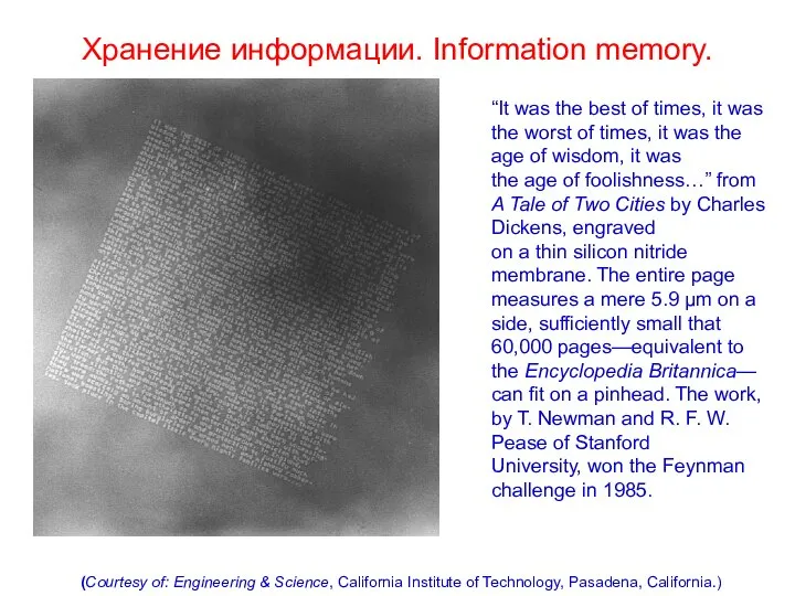
“It was the best of times, it was the worst of
“It was the best of times, it was the worst of
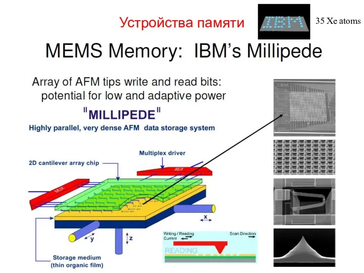
Устройства памяти
35 Xe atoms
Устройства памяти
35 Xe atoms
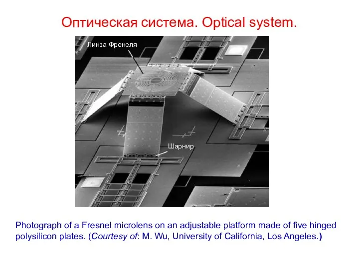
Оптическая система. Optical system.
Photograph of a Fresnel microlens on an adjustable
Оптическая система. Optical system.
Photograph of a Fresnel microlens on an adjustable
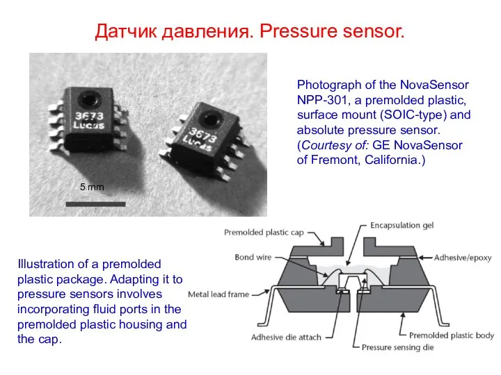
Photograph of the NovaSensor NPP-301, a premolded plastic, surface mount (SOIC-type)
Photograph of the NovaSensor NPP-301, a premolded plastic, surface mount (SOIC-type)

Photograph of a disposable blood pressure sensor for arterial-line measurement in
intensive
Photograph of a disposable blood pressure sensor for arterial-line measurement in
intensive

Преимущества Si как базового материала НЭМС
Advantages of Si in NEMS/MEMS
Дешевизна. Cheap.
Высокое
Преимущества Si как базового материала НЭМС
Advantages of Si in NEMS/MEMS
Дешевизна. Cheap.
Высокое
Формы и содинения кремния. Si forms and compounds.
Crystalline silicon is a
Формы и содинения кремния. Si forms and compounds.
Crystalline silicon is a
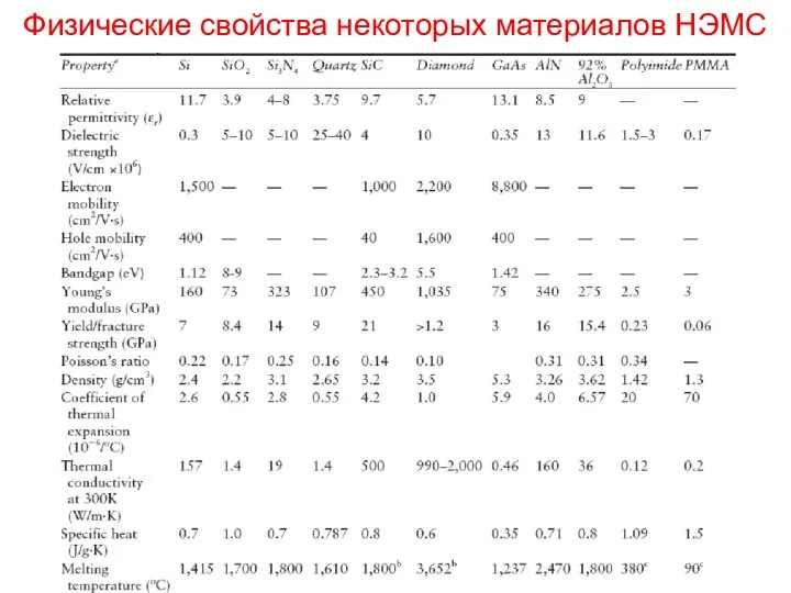
Физические свойства некоторых материалов НЭМС
Физические свойства некоторых материалов НЭМС
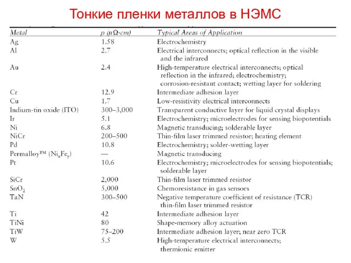
Тонкие пленки металлов в НЭМС
Тонкие пленки металлов в НЭМС
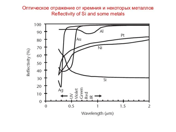
Оптическое отражение от кремния и некоторых металлов
Reflectivity of Si and some
Оптическое отражение от кремния и некоторых металлов Reflectivity of Si and some

Области применения различных материалов в НЭМС. Application areas of MEMS materials.
Области применения различных материалов в НЭМС. Application areas of MEMS materials.
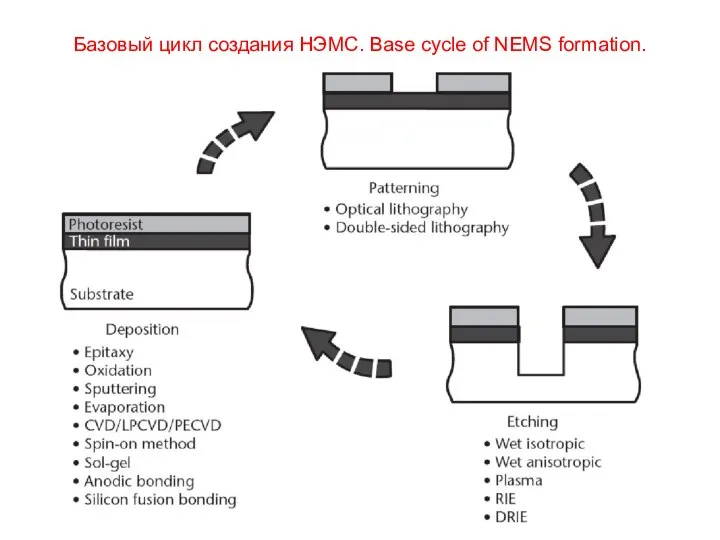
Базовый цикл создания НЭМС. Base cycle of NEMS formation.
Базовый цикл создания НЭМС. Base cycle of NEMS formation.
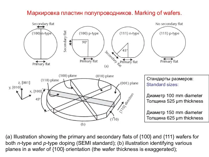
Маркировка пластин полупроводников. Marking of wafers.
(a) Illustration showing the primary and
Маркировка пластин полупроводников. Marking of wafers.
(a) Illustration showing the primary and
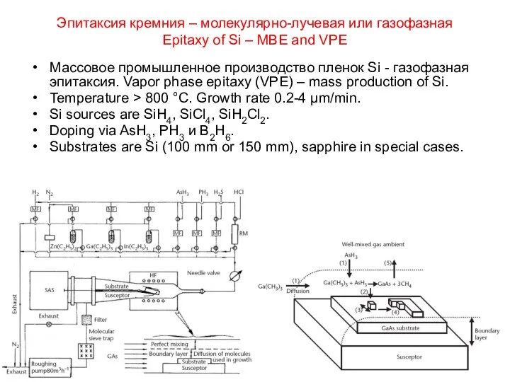
Эпитаксия кремния – молекулярно-лучевая или газофазная
Epitaxy of Si – MBE and
Эпитаксия кремния – молекулярно-лучевая или газофазная Epitaxy of Si – MBE and
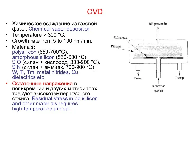
CVD
Химическое осаждение из газовой фазы. Chemical vapor deposition
Temperature > 300 °C.
Growth
CVD
Химическое осаждение из газовой фазы. Chemical vapor deposition
Temperature > 300 °C.
Growth
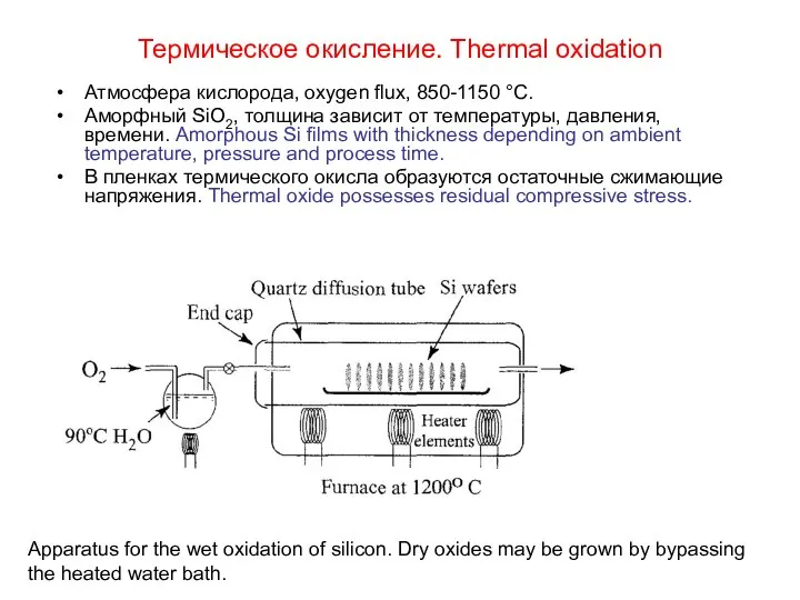
Термическое окисление. Thermal oxidation
Атмосфера кислорода, oxygen flux, 850-1150 °С.
Аморфный SiO2, толщина
Термическое окисление. Thermal oxidation
Атмосфера кислорода, oxygen flux, 850-1150 °С.
Аморфный SiO2, толщина
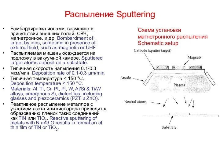
Распыление Sputtering
Бомбардировка ионами, возможно в присутствии внешних полей: СВЧ, магнетронное, и
Распыление Sputtering
Бомбардировка ионами, возможно в присутствии внешних полей: СВЧ, магнетронное, и
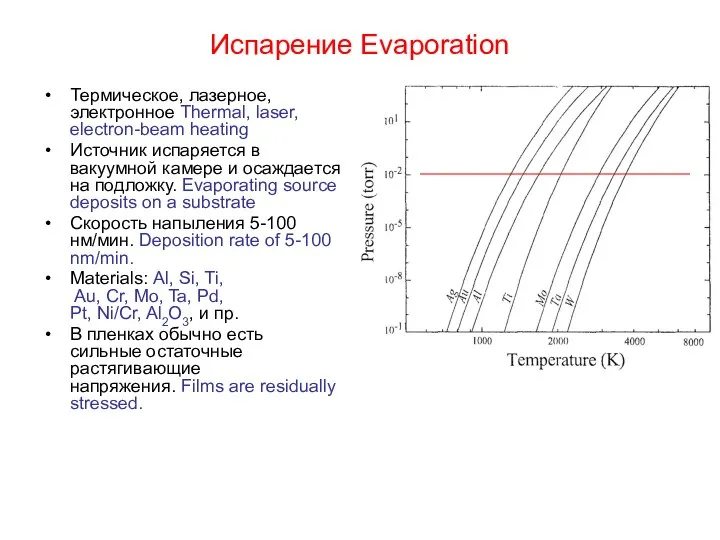
Испарение Evaporation
Термическое, лазерное, электронное Thermal, laser, electron-beam heating
Источник испаряется в вакуумной
Испарение Evaporation
Термическое, лазерное, электронное Thermal, laser, electron-beam heating
Источник испаряется в вакуумной
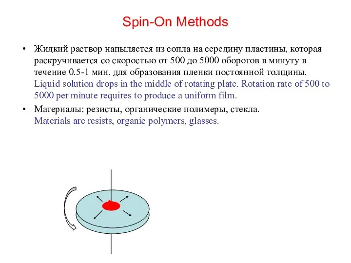
Spin-On Methods
Жидкий раствор напыляется из сопла на середину пластины, которая раскручивается
Spin-On Methods
Жидкий раствор напыляется из сопла на середину пластины, которая раскручивается
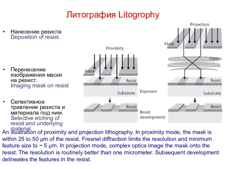
Литография Litogrophy
Нанесение резиста
Deposition of resist.
Перенесение изображения маски на резист.
Imaging mask on
Литография Litogrophy
Нанесение резиста
Deposition of resist.
Перенесение изображения маски на резист.
Imaging mask on

Фотолитография. Photolithography.
Фотолитография. Photolithography.

Lift-off метод
Ппенка напыляется на профиль резиста. Резист удаляется вместе с нанесенной
Lift-off метод
Ппенка напыляется на профиль резиста. Резист удаляется вместе с нанесенной
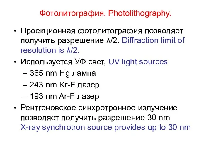
Фотолитография. Photolithography.
Проекционная фотолитография позволяет получить разрешение λ/2. Diffraction limit of resolution
Фотолитография. Photolithography.
Проекционная фотолитография позволяет получить разрешение λ/2. Diffraction limit of resolution
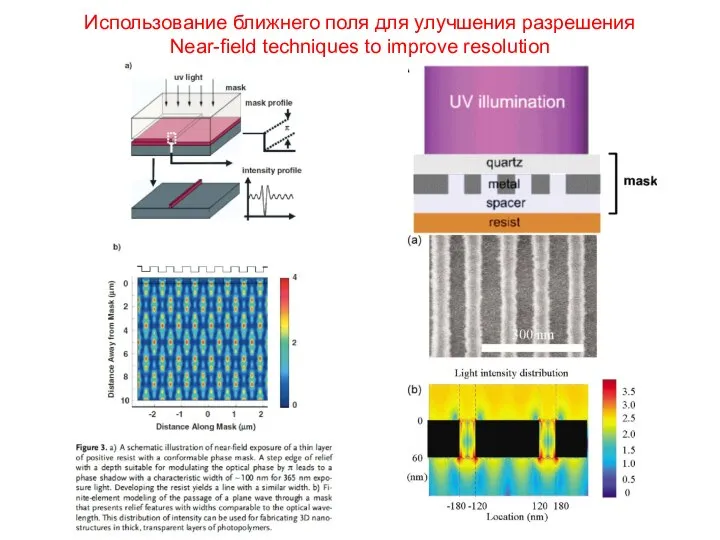
Использование ближнего поля для улучшения разрешения
Near-field techniques to improve resolution
Использование ближнего поля для улучшения разрешения
Near-field techniques to improve resolution
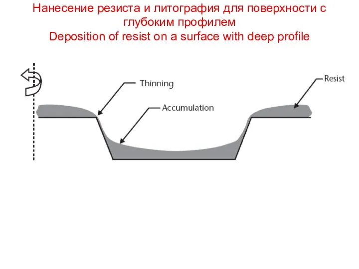
Нанесение резиста и литография для поверхности с глубоким профилем
Deposition of resist
Нанесение резиста и литография для поверхности с глубоким профилем Deposition of resist
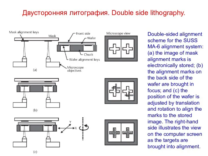
Двусторонняя литография. Double side lithography.
Double-sided alignment scheme for the SUSS MA-6
Двусторонняя литография. Double side lithography.
Double-sided alignment scheme for the SUSS MA-6

Литография с помощью электронных пучков
Electron beam lithography
Холодная полевая эмиссия электронов Шоттки.
Литография с помощью электронных пучков
Electron beam lithography
Холодная полевая эмиссия электронов Шоттки.

Сфокусированные ионные пучки
Focused ion beams
Альтернатива электронной литографии
Alternative to electron beam lithography
Нет
Сфокусированные ионные пучки
Focused ion beams
Альтернатива электронной литографии
Alternative to electron beam lithography
Нет
Scanned-Probe Lithography
AFM and STM
Resolution 1-100 nm
No mask
Limited writing rate
Scanned-Probe Lithography
AFM and STM
Resolution 1-100 nm
No mask
Limited writing rate
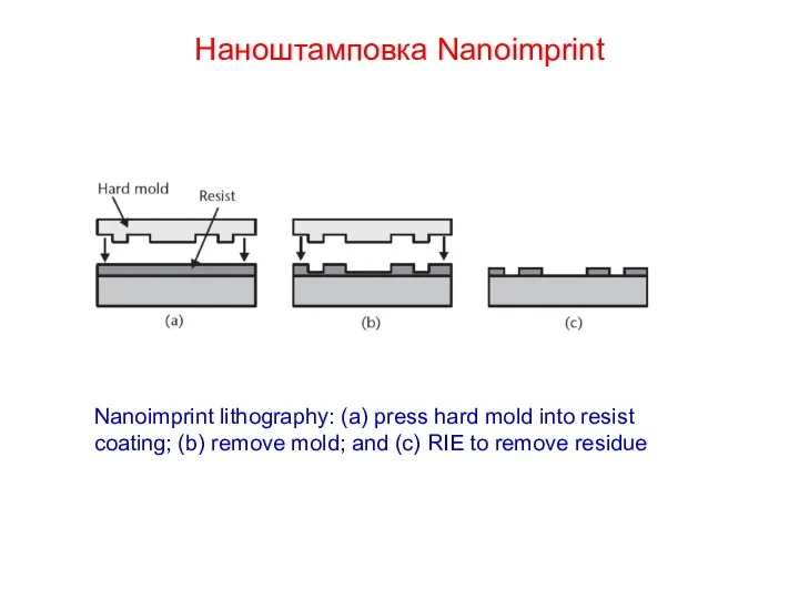
Наноштамповка Nanoimprint
Nanoimprint lithography: (a) press hard mold into resist coating; (b)
Наноштамповка Nanoimprint
Nanoimprint lithography: (a) press hard mold into resist coating; (b)
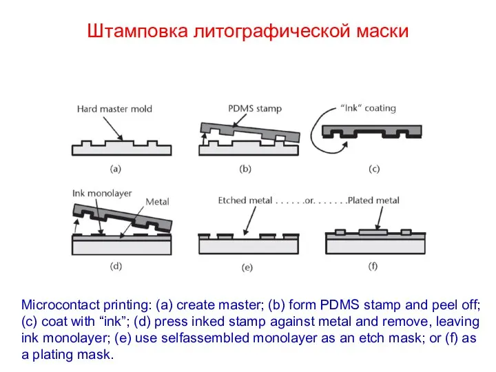
Штамповка литографической маски
Microcontact printing: (a) create master; (b) form PDMS stamp
Штамповка литографической маски
Microcontact printing: (a) create master; (b) form PDMS stamp
Заключение Conclusion
Базовым материалом НЭМС является кремний
Si is the material of choice
Заключение Conclusion
Базовым материалом НЭМС является кремний Si is the material of choice
 Специальная теория относительности. Лекция 6
 Аттестационная работа. Элективный курс "Избранные вопросы физики" в 10 классе
 Дальність дії радіолокатора
 Сила. Сила тяжести (7 класс)
 Основные характеристики атомных ядер. (Тема 1.1)
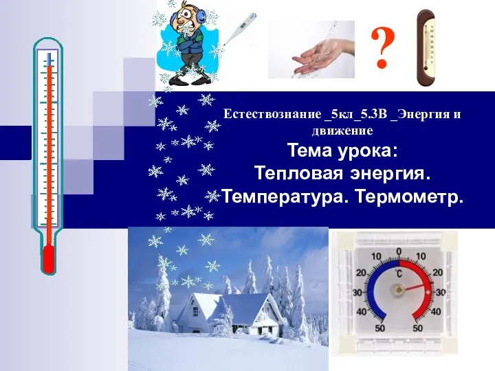 Тепловая энергия. Температура. Термометр
 Молекулярная физика и термодинамика
 Табиғи үдерістерді физика, химия, механика, тағы басқа жаратылыстану ғылымдары зерттейді
 Бензиновые двигатели с непосредственным впрыском АВ120
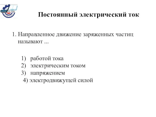 Постоянный электрический ток
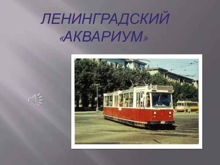 Ленинградский Аквариум
 Джерела і приймачі світла. Поглощеня і розсіювання світла
 Воздействие лазерного излучения на мишени
 Вопросы Что такое магнитная проницаемость? Какие вещества называют диа- и парамагнетиками? Что такое ферромагнетики? Каковы
  Физические свойства строительных материалов
 Расчет участка контактной сети однофазного переменного тока. Специальная часть: монтаж устройств освещения объектов
 Ремонт охлаждающей и смазочной систем двигателей
 РАСЧЁТ И КОНСТРУИРОВАНИЕ БАЗЫ КОЛОННЫ
  Горение электрической дуги
 Демонстрационный вариант контрольных измерительных материалов единого государственного экзамена 2015 года по физике
 Презентация Электроемкость. Конденсаторы
 Аэродинамика полосок бумаги или И все-таки она вертится!.. Белецкий антон 4 «г» класс МАОУ лицей №28 г.Таганрога
  Процесстер мен аппараттар
 Атмосферное давление на разных высотах. Манометры
 Расчет сопротивления проводника. Удельное сопротивление
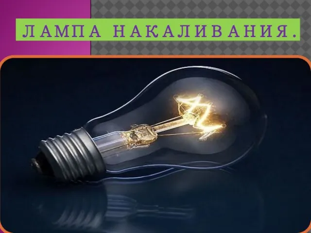 Лампа накаливания
 Сила трения. 7 класс
 Газовые законы. Основное уравнение состояния газа