- 2012 Component Training Ivy Platform Series

Содержание
- 2. Platform Structure CPU feature introduce Intel 7 series chipset architecture Critical Power Flow Clock Distribution Power
- 8. Platform Structure CPU feature introduce Intel 7 series chipset architecture Critical Power Flow Clock Distribution Power
- 11. Platform Structure CPU feature introduce Intel 7 series chipset architecture Critical Power Flow Clock Distribution Power
- 12. 7 Series due to over clocking, Z77&H77 series MB have some difference: Z77 series MB all
- 13. : Can measure the waveform
- 14. 1. If PCH internal provide CLK, it will use two 10K ohm resistors to connect to
- 15. To 14M_PCH Check point: VCC 14M crystal CK_PG CK_RESET# Refer model: P8H77-V LE
- 16. Platform Structure CPU feature introduce Intel 7 series chipset architecture Critical Power Flow Clock Distribution Power
- 17. SIO 3V_ATX +BAT_3V SR107 S_DSWVRMEN Power Supply S_RTCRST# O_RSMRST# O2_RSMRST# 1 2 3 4 6 SR106
- 18. SIO Power Button O_PWRBTN#IN O_PWRBTN# SIO SLP_S3# SLP_S4# O_PSON# O2_CUT_PSON# O2_PSON# Power Supply O2_PSON# 3V, 5V,
- 20. Platform Structure CPU feature introduce Intel 7 series chipset architecture Critical Power Flow Clock Distribution Power
- 21. +3VSB_ATX +3VSB_ATX PWRBTN# PANEL (B) 1. Check SIO power sequence and working condition: SIO PCH O_PWRBTN#_R
- 22. 2. Check PCH power sequence and working condition 3. Other condition: make sure 5V_DUAL & 1.5VDUAL
- 23. 4. O_SKTOCC: SIO uses this pin to detect MB with CPU or not. At G3, before
- 24. Update BIOS or exchange another BIOS chipset Make sure that MB has no crack, trace open
- 25. +3VSB_ATX +3VSB_ATX PWRBTN# PANEL (B) SIO PCH O_PWRBTN#_R (C) O_IOPWRBTN# (D) SLP_S3# (E) SLP_S4# (E) RSMRST#
- 26. If PCH working condition is abnormal, MB also will shutdown. PCH 1.05ME 1.05PCH 1.8VSFR VCCIO 3V
- 27. Problem with power shutdown: THERMAL signals, voltage, PCH working condition and the power sequence (power ok
- 28. After 00 and CPURST#: CPU to PCH (DMI) PCH to BIOS (SPI) SPI to PCH (SPI)
- 29. Measure BUS: DMI: H_DMI_RXN/P[0:3] H_DMI_TXN/P[0:3] S_DMICOMP S_DMIRBIAS VCCDMI_PLL_PCH SMB: S_SMBCLK_MAIN S_SMBDATA_MAIN S_SMBCLK_PCI S_SMBDATA_PCI Memory to CPU
- 30. LPC SMBUS CLOCK PWM ADC FAN OP_MODE Control O2_VREF 3VSB O2_VDDA (O2_3.2V) EC C.SEPT036 24M Crystal
- 31. Refer model: P8Z77-V LE Intel input voltage Output voltage Chipset (EC C.SKB3722)
- 32. Refer model: P8Z77-V LE EC of S3, S4 signals will change with different status. Before boot
- 33. Measure CPU voltage: VCORE, GFX, VCCIO, VCCSA, 1.8SFR, 1.5VDUAL Check 12V, 3V, 3VSB on PCIEX slot.
- 34. FDI and DMI Bus, make sure that all LED lights are normal CPU voltage: VCORE, GFX,
- 35. Vcc=3.3V Vinsen = 0.86V VRHot = Vcc EN=3.3V Sequence 1.2.3 first En signal V18A= 1.8V
- 36. Vcc= 5V DVD= 1.5V≧1.11 DVDA = 1.33V≧1.11 EN= VCCIO≒1.05 Sequence 1.2.3 first EN signal ASP1000RM
- 37. Vcc5= 5V Vcc12= 12V EN=VCCIO≒ 1.05V Sequence 1.2 first EN signal ASP1102
- 38. ASP0A13
- 39. IR8510
- 40. Vcore voltage output of each phase must have the correct waveform Empty board boot to Vcore
- 41. If you suspect that other components are burned, such as the Driver To see whether the
- 42. high low Clear COMS and let MB at load default status Check +5VSB_ATX Check O_DEEPS5 and
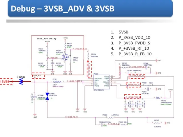
- 43. 5VSB P_3VSB_VDD_10 P_3VSB_PVDD_S P_+3VSB_RT_10 P_3VSB_R_FB_10 3VSB 0 ohm
- 44. high low low low high low Check O_3VSBSW# (At S0 and S5 status, this signal has
- 45. 5VDUAL and PU501 VCC Check P_1V5DUAL_OCSET/EN_10 Check MOS Check P_1V5DUAL_FB_10 has 0.8V Check NCT3933 working condition
- 46. 8.2K ohm 25.5 K ohm Low
- 47. 3VSB 3VSB 10K 11.5 K 10 K 26.1 K P_1V8_SFR_IN+_10 P_VCCSA_IN+_10 4.7 K ohm 4.7 K
- 49. Скачать презентацию
Platform Structure
CPU feature introduce
Intel 7 series chipset architecture
Critical Power Flow
Clock Distribution
Power
Platform Structure
CPU feature introduce
Intel 7 series chipset architecture
Critical Power Flow
Clock Distribution
Power


Platform Structure
CPU feature introduce
Intel 7 series chipset architecture
Critical Power Flow
Clock Distribution
Power
Platform Structure
CPU feature introduce
Intel 7 series chipset architecture
Critical Power Flow
Clock Distribution
Power

Platform Structure
CPU feature introduce
Intel 7 series chipset architecture
Critical Power Flow
Clock Distribution
Power
Platform Structure
CPU feature introduce
Intel 7 series chipset architecture
Critical Power Flow
Clock Distribution
Power
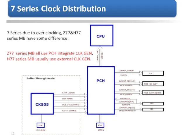
7 Series due to over clocking, Z77&H77 series MB have some
7 Series due to over clocking, Z77&H77 series MB have some
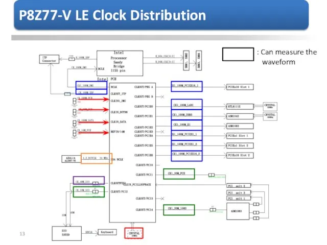
: Can measure the
waveform
: Can measure the
waveform
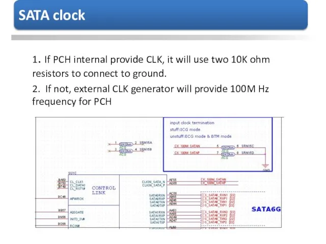
1. If PCH internal provide CLK, it will use two 10K
1. If PCH internal provide CLK, it will use two 10K
To 14M_PCH
Check point:
VCC
14M crystal
CK_PG
CK_RESET#
Refer model: P8H77-V LE
To 14M_PCH
Check point:
VCC
14M crystal
CK_PG
CK_RESET#
Refer model: P8H77-V LE
Platform Structure
CPU feature introduce
Intel 7 series chipset architecture
Critical Power Flow
Clock Distribution
Power
Platform Structure
CPU feature introduce
Intel 7 series chipset architecture
Critical Power Flow
Clock Distribution
Power
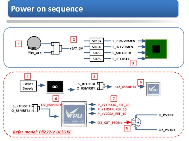
SIO
3V_ATX
+BAT_3V
SR107
S_DSWVRMEN
Power Supply
S_RTCRST#
O_RSMRST#
O2_RSMRST#
1
2
3
4
6
SR106
S_INTVRMEN
SR79
S_SRTCRST#
SR75
S_RTCRST#
5
S_RTCRST #
O2_RSMRST#
P_+VTTCCIO_REF_10
P_+1.8SFR_REF_10
P_+VCCSA_REF_10
O_RSMRST#
O2_CUT_PSON#
O_PSON#
O2_PSON#
8
6
7
Refer model: P8Z77-V DELUXE
SIO
3V_ATX
+BAT_3V
SR107
S_DSWVRMEN
Power Supply
S_RTCRST#
O_RSMRST#
O2_RSMRST#
1
2
3
4
6
SR106
S_INTVRMEN
SR79
S_SRTCRST#
SR75
S_RTCRST#
5
S_RTCRST #
O2_RSMRST#
P_+VTTCCIO_REF_10
P_+1.8SFR_REF_10
P_+VCCSA_REF_10
O_RSMRST#
O2_CUT_PSON#
O_PSON#
O2_PSON#
8
6
7
Refer model: P8Z77-V DELUXE
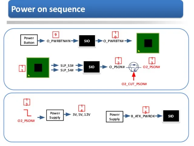
SIO
Power Button
O_PWRBTN#IN
O_PWRBTN#
SIO
SLP_S3#
SLP_S4#
O_PSON#
O2_CUT_PSON#
O2_PSON#
Power Supply
O2_PSON#
3V, 5V, 12V
Power Supply
B_ATX_PWROK
SIO
10
9
11
12
13
13
14
15
SIO
Power Button
O_PWRBTN#IN
O_PWRBTN#
SIO
SLP_S3#
SLP_S4#
O_PSON#
O2_CUT_PSON#
O2_PSON#
Power Supply
O2_PSON#
3V, 5V, 12V
Power Supply
B_ATX_PWROK
SIO
10
9
11
12
13
13
14
15

Platform Structure
CPU feature introduce
Intel 7 series chipset architecture
Critical Power Flow
Clock Distribution
Power
Platform Structure
CPU feature introduce
Intel 7 series chipset architecture
Critical Power Flow
Clock Distribution
Power
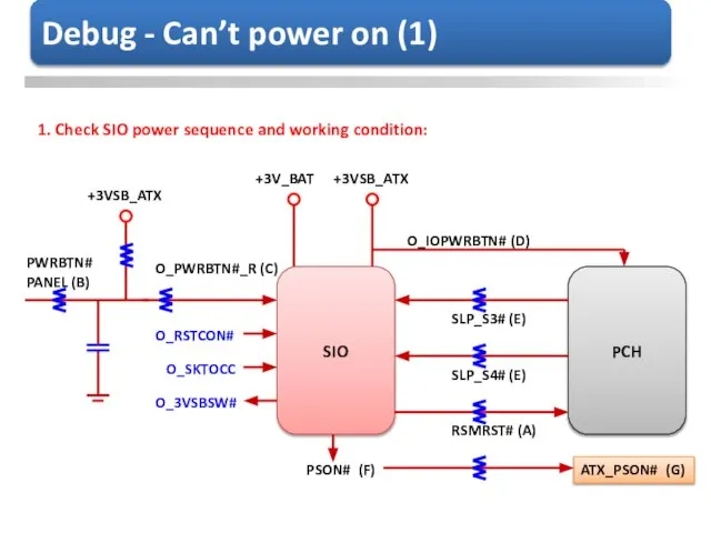
+3VSB_ATX
+3VSB_ATX
PWRBTN#
PANEL (B)
1. Check SIO power sequence and working condition:
SIO
PCH
O_PWRBTN#_R (C)
O_IOPWRBTN# (D)
SLP_S3#
+3VSB_ATX
+3VSB_ATX
PWRBTN#
PANEL (B)
1. Check SIO power sequence and working condition:
SIO
PCH
O_PWRBTN#_R (C)
O_IOPWRBTN# (D)
SLP_S3#
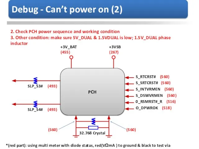
2. Check PCH power sequence and working condition
3. Other condition: make
2. Check PCH power sequence and working condition 3. Other condition: make
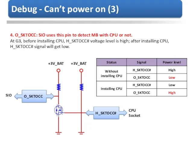
4. O_SKTOCC: SIO uses this pin to detect MB with CPU
4. O_SKTOCC: SIO uses this pin to detect MB with CPU
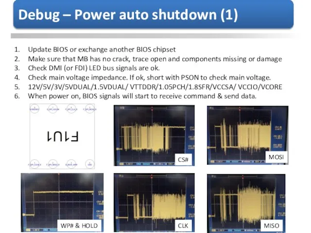
Update BIOS or exchange another BIOS chipset
Make sure that MB has
Update BIOS or exchange another BIOS chipset
Make sure that MB has
+3VSB_ATX
+3VSB_ATX
PWRBTN#
PANEL (B)
SIO
PCH
O_PWRBTN#_R (C)
O_IOPWRBTN# (D)
SLP_S3# (E)
SLP_S4# (E)
RSMRST# (A)
PSON# (F)
+3V_BAT
O_RSTCON#
ATX_PSON# (G)
O_SKTOCC
O_3VSBSW#
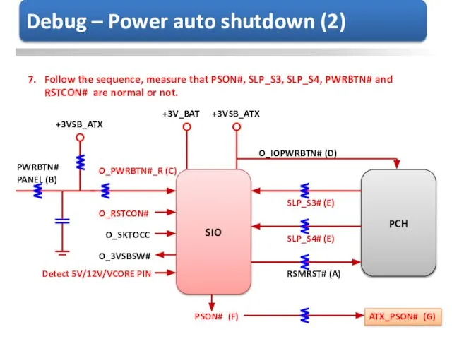
7. Follow the sequence,
+3VSB_ATX
+3VSB_ATX
PWRBTN#
PANEL (B)
SIO
PCH
O_PWRBTN#_R (C)
O_IOPWRBTN# (D)
SLP_S3# (E)
SLP_S4# (E)
RSMRST# (A)
PSON# (F)
+3V_BAT
O_RSTCON#
ATX_PSON# (G)
O_SKTOCC
O_3VSBSW#
7. Follow the sequence,
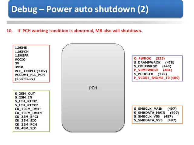
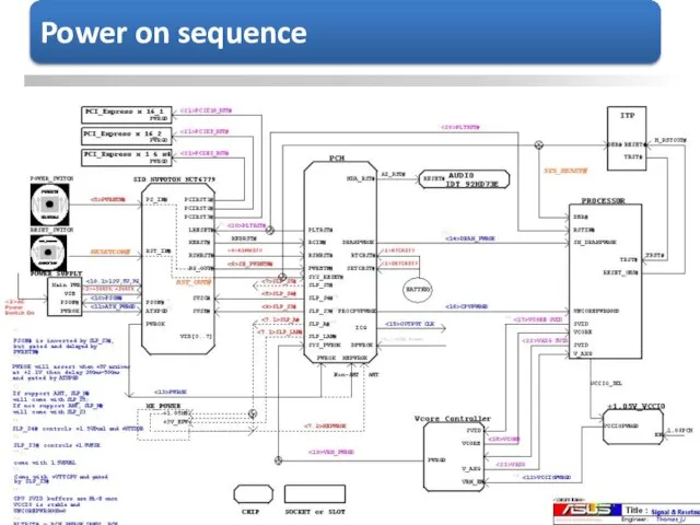
If PCH working condition is abnormal, MB also will shutdown.
PCH
1.05ME
1.05PCH
1.8VSFR
VCCIO
3V
3VSB
VCC_XCKPLL (1.8V)
VCCDMI_PLL_PCH
(1.05~1.1V)
S_25M_OUT
S_25M_IN
S_ICH_RTCX1
S_ICH_RTCX2
CK_100M_DMIP
CK_100M_DMIN
CK_33M_EPCI
CK_33M_SIO
CK_33M_PCH
CK_48M_SIO
O_PWROK
If PCH working condition is abnormal, MB also will shutdown.
PCH
1.05ME
1.05PCH
1.8VSFR
VCCIO
3V
3VSB
VCC_XCKPLL (1.8V)
VCCDMI_PLL_PCH
(1.05~1.1V)
S_25M_OUT
S_25M_IN
S_ICH_RTCX1
S_ICH_RTCX2
CK_100M_DMIP
CK_100M_DMIN
CK_33M_EPCI
CK_33M_SIO
CK_33M_PCH
CK_48M_SIO
O_PWROK
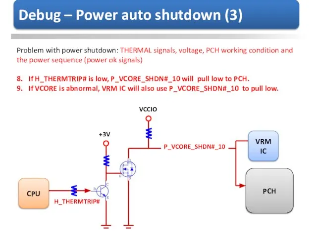
Problem with power shutdown: THERMAL signals, voltage, PCH working condition and
the
Problem with power shutdown: THERMAL signals, voltage, PCH working condition and
the
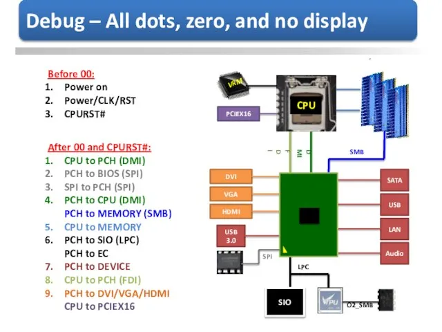
After 00 and CPURST#:
CPU to PCH (DMI)
PCH to BIOS (SPI)
SPI to
After 00 and CPURST#:
CPU to PCH (DMI)
PCH to BIOS (SPI)
SPI to
![Measure BUS: DMI: H_DMI_RXN/P[0:3] H_DMI_TXN/P[0:3] S_DMICOMP S_DMIRBIAS VCCDMI_PLL_PCH SMB: S_SMBCLK_MAIN S_SMBDATA_MAIN](/_ipx/f_webp&q_80&fit_contain&s_1440x1080/imagesDir/jpg/559719/slide-28.jpg)
Measure BUS:
DMI:
H_DMI_RXN/P[0:3]
H_DMI_TXN/P[0:3]
S_DMICOMP
S_DMIRBIAS
VCCDMI_PLL_PCH
SMB:
S_SMBCLK_MAIN
S_SMBDATA_MAIN
S_SMBCLK_PCI
S_SMBDATA_PCI
Memory to CPU
D3A_DQ[0:63]
D3A_MA[0:15]
D3A_DQSN/P[0:7]
D3A_BA[0:2]
D3_RESET#
FDI:
H_FDI_INT
H_FDI_COMP
H_FDI_FSYNC[0:1]
H_FDI_LSYNC[0:1]
H_FDI_TXN/P[0:7]
D3A_CLKP/N[0:1]
D3A_CS#[0:1]
D3A_ODT[0:1]
D3A_CKE[0:1]
D3A_WE#
D3A_RAS#
D3A_CAS#
LPC
SMBUS
CLOCK
PWM
ADC
FAN
OP_MODE
Control
O2_VREF
3VSB
O2_VDDA (O2_3.2V)
EC
C.SEPT036
24M Crystal
F_FRAME#
F_SERIRQ#
F_LAD [0:3]
C_PCI_EC
S_PLTRST
O2_SMB1_CLK/DATA
O2_SMB2_CLK/DATA
O2_PWM1 (VCCSA)
O2_PWM2 (VCCIO)
O2_PWM3 (1.8SFR)
O2_OP_MODE
O2_AD0 (1.05PCH)
O2_AD1 (VCCIO)
O2_AD2 (1.8SFR)
O2_AD3 (1.5DUAL)
O2_SEN_CPUOPT
O2_RSMRST#
O2_CUT_PSON#
O2_VAUX_OUT
O_PWRBTN#IN_R
O2_RSTCON#_R
O2_VRMPWRGD
VRMPWRGD
S_SLPS3#/S4#
O_PWROK
J_SILENT#
Refer model: P8Z77-V DELUXE
Chipset (EC C.SEPT036)
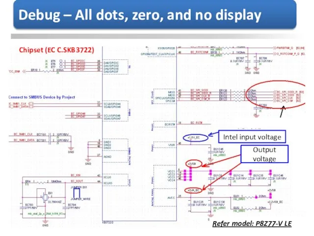
Refer model: P8Z77-V LE
Intel input voltage
Output voltage
Chipset (EC C.SKB3722)
Refer model: P8Z77-V LE
Intel input voltage
Output voltage
Chipset (EC C.SKB3722)
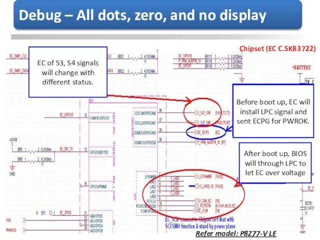
Refer model: P8Z77-V LE
EC of S3, S4 signals will change
Refer model: P8Z77-V LE
EC of S3, S4 signals will change
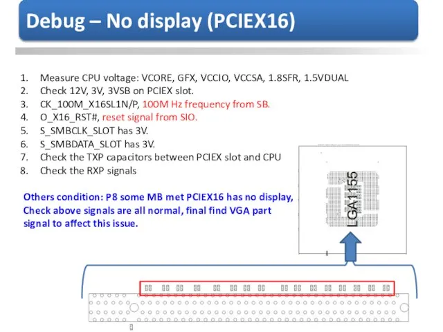
Measure CPU voltage: VCORE, GFX, VCCIO, VCCSA, 1.8SFR, 1.5VDUAL
Check 12V, 3V,
Measure CPU voltage: VCORE, GFX, VCCIO, VCCSA, 1.8SFR, 1.5VDUAL
Check 12V, 3V,
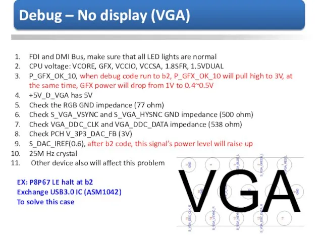
FDI and DMI Bus, make sure that all LED lights are
FDI and DMI Bus, make sure that all LED lights are
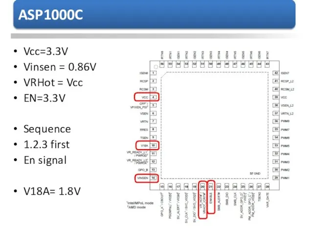
Vcc=3.3V
Vinsen = 0.86V
VRHot = Vcc
EN=3.3V
Sequence
1.2.3 first
En signal
V18A= 1.8V
Vcc=3.3V
Vinsen = 0.86V
VRHot = Vcc
EN=3.3V
Sequence
1.2.3 first
En signal
V18A= 1.8V
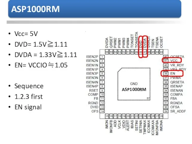
Vcc= 5V
DVD= 1.5V≧1.11
DVDA = 1.33V≧1.11
EN= VCCIO≒1.05
Sequence
1.2.3 first
EN signal
ASP1000RM
Vcc= 5V
DVD= 1.5V≧1.11
DVDA = 1.33V≧1.11
EN= VCCIO≒1.05
Sequence
1.2.3 first
EN signal
ASP1000RM
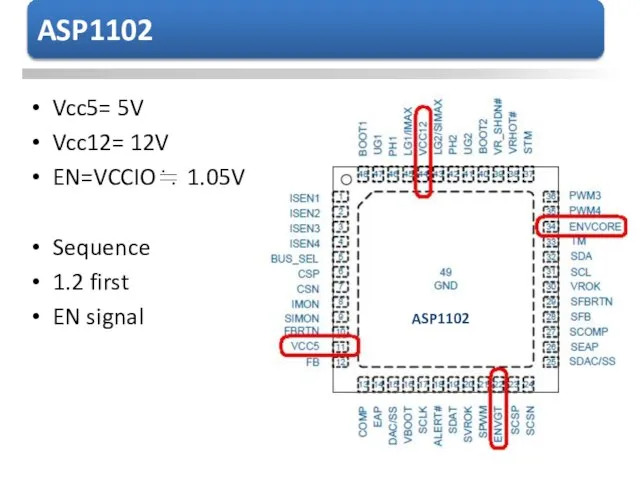
Vcc5= 5V
Vcc12= 12V
EN=VCCIO≒ 1.05V
Sequence
1.2 first
EN signal
ASP1102
Vcc5= 5V
Vcc12= 12V
EN=VCCIO≒ 1.05V
Sequence
1.2 first
EN signal
ASP1102
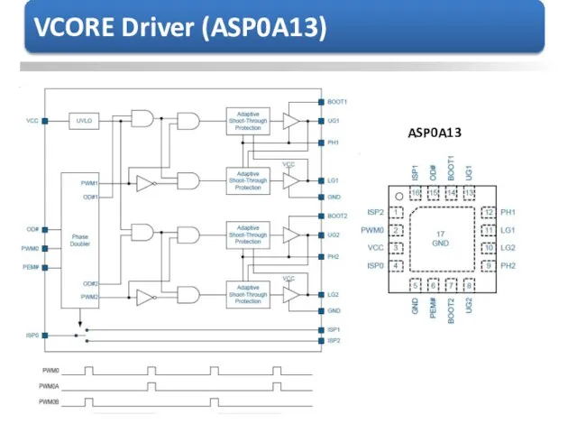
ASP0A13
ASP0A13
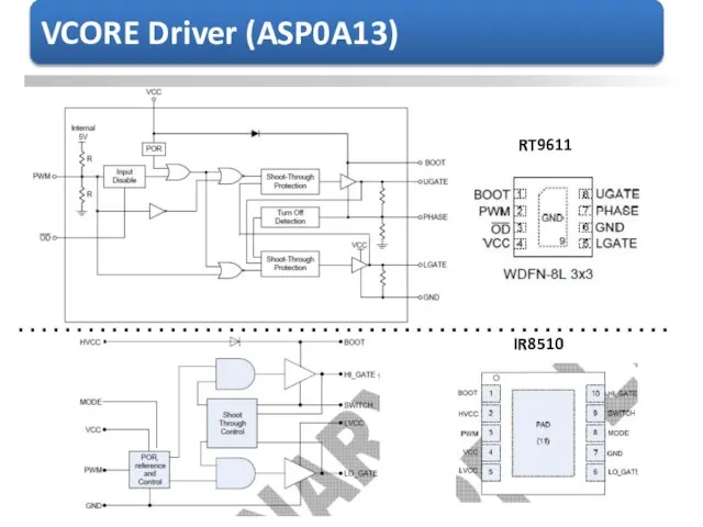
IR8510
IR8510
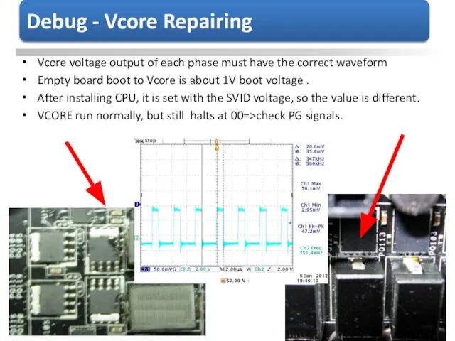
Vcore voltage output of each phase must have the correct waveform
Empty
Vcore voltage output of each phase must have the correct waveform
Empty
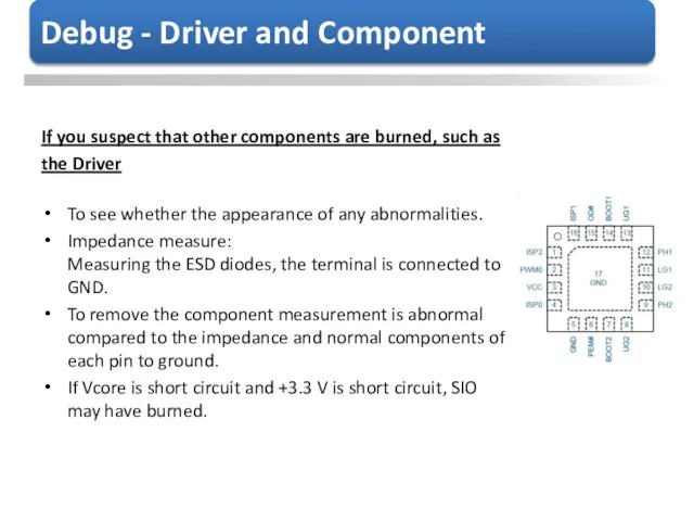
If you suspect that other components are burned, such as
the
If you suspect that other components are burned, such as
the
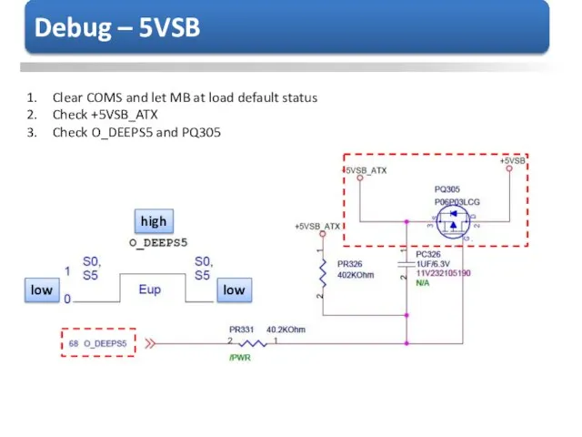
high
low
Clear COMS and let MB at load default status
Check +5VSB_ATX
Check O_DEEPS5
high
low
Clear COMS and let MB at load default status
Check +5VSB_ATX
Check O_DEEPS5
5VSB
P_3VSB_VDD_10
P_3VSB_PVDD_S
P_+3VSB_RT_10
P_3VSB_R_FB_10
3VSB
0 ohm
5VSB
P_3VSB_VDD_10
P_3VSB_PVDD_S
P_+3VSB_RT_10
P_3VSB_R_FB_10
3VSB
0 ohm
high
low
low
low
high
low
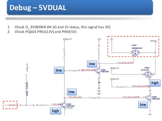
Check O_3VSBSW# (At S0 and S5 status, this signal has 3V)
Check
high
low
low
low
high
low
Check O_3VSBSW# (At S0 and S5 status, this signal has 3V)
Check
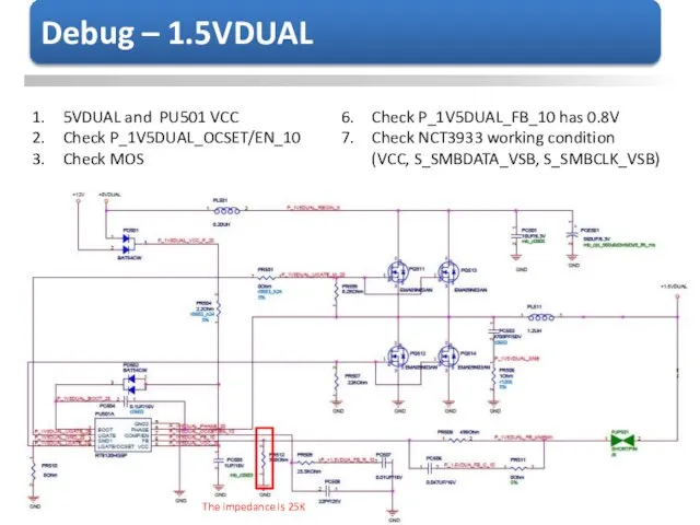
5VDUAL and PU501 VCC
Check P_1V5DUAL_OCSET/EN_10
Check MOS
Check P_1V5DUAL_FB_10 has 0.8V
Check NCT3933
5VDUAL and PU501 VCC
Check P_1V5DUAL_OCSET/EN_10
Check MOS
Check P_1V5DUAL_FB_10 has 0.8V
Check NCT3933
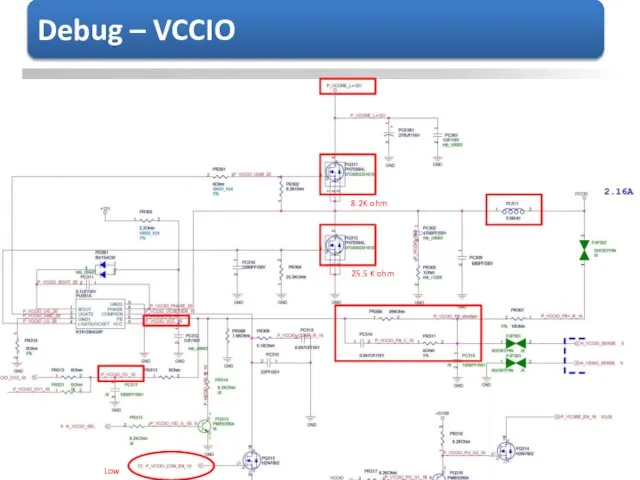
8.2K ohm
25.5 K ohm
Low
8.2K ohm
25.5 K ohm
Low
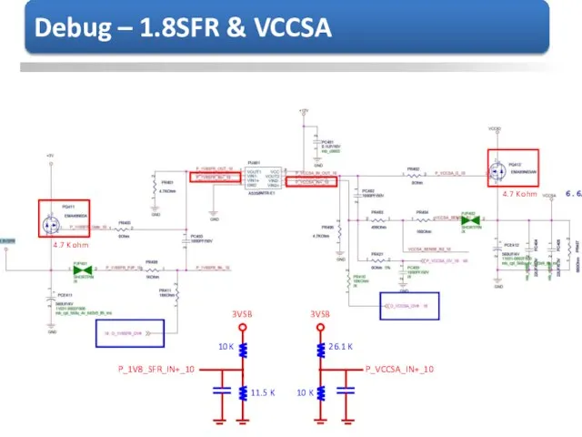
3VSB
3VSB
10K
11.5 K
10 K
26.1 K
P_1V8_SFR_IN+_10
P_VCCSA_IN+_10
4.7 K ohm
4.7 K
3VSB
3VSB
10K
11.5 K
10 K
26.1 K
P_1V8_SFR_IN+_10
P_VCCSA_IN+_10
4.7 K ohm
4.7 K
 1С:Медицина. Стоматологическая клиника
 Задачи SCADA-систем и их решение в программных комплексах
 Создание Web-страниц на языке HTML
 CRM-приложения, обеспечивающие работу электронного правительства
 Create a own Database
 Цифровая культура
 Файловая структура компьютера
 Event Sourcing
 Актуальность информационной безопасности детей
 Основы WLAN
 Архитектура ORACLE. Процессы и потоки Windows (Лекция 6)
 Язык программирования SAS Base
 Моделирование, как метод познания. Общие свойства моделей
 Консоль или ПК?
 О кассах, маркировке ЭДО и электронных подписях
 Технологии программирования. Курс на базе Microsoft Solutions Framework Семинар 1. Повтор принципов объектно-ориентированного подхода
  Требования к оформлению. Межвузовские, региональные, отборочные чемпионаты
 Grafka i komunikacja człowieka z komputerem
 Программирование на языке fbd codesys
 Массивы. Лекция 5
 Работа с информацией
 Учебный курс Введение в цифровую электронику Лекция 4 Основные понятия микропроцессорной техники кандидат технических н
 Урок информатики 5 класс
 Хранение информации Память человека и память человечества Оперативная и долговременная память Файлы и папки Это интересно
 Компьютерные вирусы и антивирусные программы
 Компьютерные средства управления технологическими процессами
 Зачем вам блог
 Итак, представляю вам последнюю разработку корпорации Microsoft: Windows Vista