- High-Density Ac-Dc Power Supplies using Active-Clamp Flyback Topologу

Содержание
- 2. Agenda Introduction to active-clamp flyback operation (ACF) ACF light-load efficiency challenge Introduction to the NCP1568 –
- 3. Introduction to Active-Clamp Flyback Operation (ACF)
- 4. Active-Clamp Flyback The clamp diode in a standard flyback converter is replaced by a switch hence
- 5. Why Active-Clamp Flyback? Zero-Volt Switching of the FETs with Fixed-Switching Frequency Results in high switching frequency,
- 6. Energy-Storage Mode The energy-storage mode is similar to that of a classical flyback converter: when the
- 7. Transition from Energy-Storage Mode to Power-Delivery Mode When FET turns off, the lump capacitor on the
- 8. Power-Delivery Mode In this mode, Lleak resonates with clamp capacitor (Cclamp). The resonant frequency is given
- 9. Transition from Power-Delivery Mode to Energy-Storage Mode When the clamp FET turns off, Lleak resonates with
- 10. Leakage Inductance Needed for ZVS For universal design, leakage inductance needed to get ZVS increases in
- 11. ZVS Phenomenon – 1 During Tdis1 (shaded region), Lleak resonates with Cclamp. The time it takes
- 12. ZVS Phenomenon – 2 During Tdis2 (shaded region), negative magnetizing current starts to discharge the clamp
- 13. Fixed-Frequency Operation Magnetizing current in ACF is in CCM. As the load current decreases, the valley
- 14. Variable-Frequency Operation As the load current decreases, increasing the frequency minimizes Imag and reduces the conduction
- 15. Light-Load Efficiency & Standby Power Challenge
- 16. Light-Load Efficiency Requirements European Code of Conduct, Ver. 5, Tier 2 poses stringent efficiency standards at
- 17. Standby Power Standard US DoE standards are equally stringent Most of the brand name OEMs require
- 18. ACF Specific Light-Load Challenges Magnetizing current is in CCM. Frequency modulation results in high-frequency operation at
- 19. DCM Operation Holding active-clamp FET off, DCM operation can be implemented in ACF. This allows magnetizing
- 20. Introduction to NCP1568 Ac-Dc PWM Controller for ACF
- 21. Introduction to NCP1568 Control Scheme Adaptive ZVS frequency modulation allows variable Vout operation Integrated adaptive dead-time
- 22. Frequency Movement vs. Load NCP1568 NCP1568 features a combination of nonlinear & linear foldback schemes The
- 23. Clamp Capacitor Challenge VCLAMP_DCM>VCLAMP_ACF Leakage energy is not recycled in DCM and is dissipated in the
- 24. Transition from DCM to ACF Active-clamp FET can be soft-started to discharge the clamp capacitor slowly.
- 25. DCM Operation Determination NCP1568 can be configured to operate in pure ACF mode and pure DCM
- 26. Key Components Selection Transformer Design & Key Equations
- 27. Design Specifications
- 28. Turns Ratio Selection Turns ratio can be calculated by the following formula assuming Dmax=0.5. Turns ratio
- 29. Minimum On-Time Minimum on-time needs to be calculated at worst case duty ratio to ensure that
- 30. Valley Current for ZVS In order to determine the inductance value, valley current is needed. To
- 31. Inductance Calculation Inductance can be calculated as follows: Where Dmin is the minimum duty cycle given
- 32. Inductance vs. Required Valley Current for ZVS As the required valley current for ZVS decreases, the
- 33. Core Selection Assuming a 200-mT Bmax operating at 400 kHz results in a core loss of
- 34. Primary and Secondary Turns The primary and secondary turns can be calculated from the following formulae:
- 35. Clamp Capacitor Selection Clamp capacitor should be selected at worst-case off-time i.e., lowest frequency and minimum
- 36. RMS Current Formulae The primary and secondary FET selection criterion is no different than with standard
- 37. 60-W UHD-Board Performance
- 38. Simplified Schematic Secondary side is similar to any standard flyback topology.
- 39. Frequency Modulation w. Load As the load current decreases, the negative current is minimized & kept
- 40. Fixed Frequency vs. Frequency Modulation 115 V rms, 1.5-A load Fixed Fsw of 231 kHz 115
- 41. Frequency Movement w. Vout & Vin Frequency movement is similar to QR flyback switching in 1st
- 42. Frequency vs. Load Current Active-Clamp Mode Discontinuous Mode
- 43. DCM SW waveforms 90 V rms 265 V rms
- 44. NCP1568 USB PD 65-W UHD Demonstration Board Featured Devices: NCP1568 ACF Controller NCP51530 Half-Bridge Driver NCP4305
- 45. UHD Board Performance Achieving a full-load efficiency of 93.5% at a 60-W output Primary FETs running
- 46. NCP1568 Demonstration Board Efficiency
- 48. Скачать презентацию
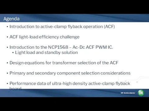
Agenda
Introduction to active-clamp flyback operation (ACF)
ACF light-load efficiency challenge
Introduction to the
Agenda
Introduction to active-clamp flyback operation (ACF)
ACF light-load efficiency challenge
Introduction to the
Introduction to
Active-Clamp Flyback Operation (ACF)
Introduction to
Active-Clamp Flyback Operation (ACF)
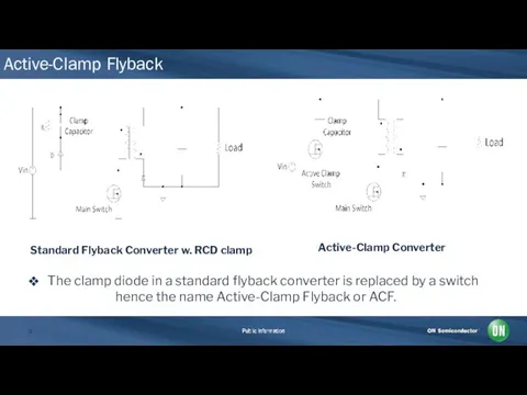
Active-Clamp Flyback
The clamp diode in a standard flyback converter is replaced
Active-Clamp Flyback
The clamp diode in a standard flyback converter is replaced
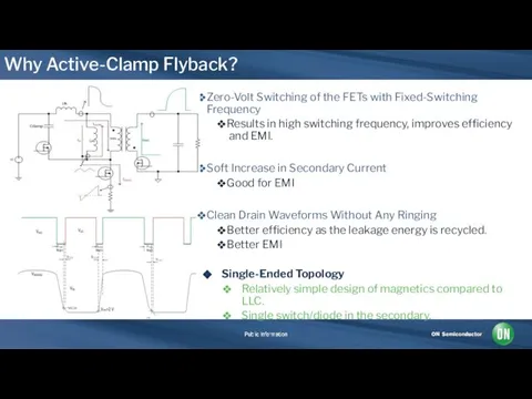
Why Active-Clamp Flyback?
Zero-Volt Switching of the FETs with Fixed-Switching Frequency
Results in
Why Active-Clamp Flyback?
Zero-Volt Switching of the FETs with Fixed-Switching Frequency
Results in
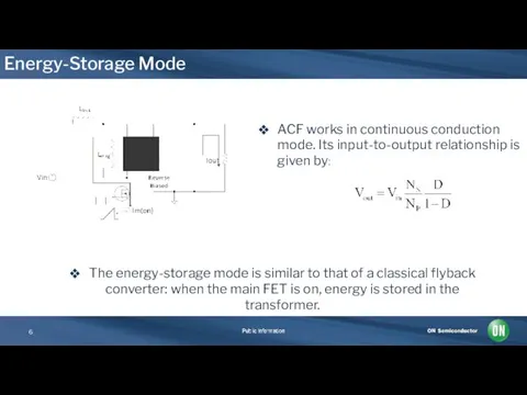
Energy-Storage Mode
The energy-storage mode is similar to that of a classical
Energy-Storage Mode
The energy-storage mode is similar to that of a classical
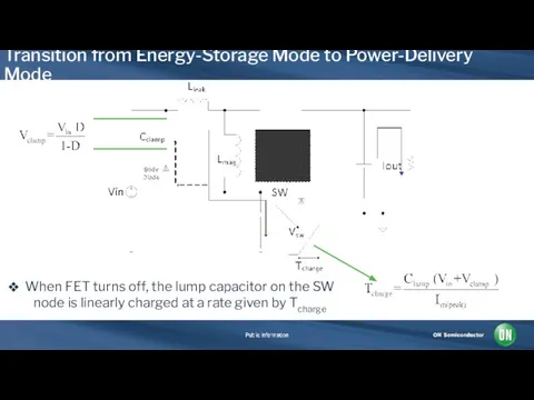
Transition from Energy-Storage Mode to Power-Delivery Mode
When FET turns off, the
Transition from Energy-Storage Mode to Power-Delivery Mode
When FET turns off, the
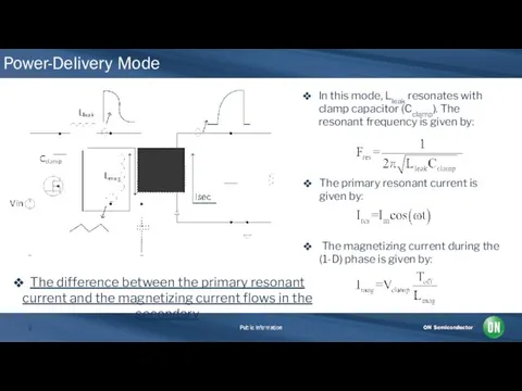
Power-Delivery Mode
In this mode, Lleak resonates with clamp capacitor (Cclamp). The
Power-Delivery Mode
In this mode, Lleak resonates with clamp capacitor (Cclamp). The
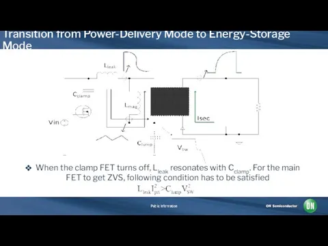
Transition from Power-Delivery Mode to Energy-Storage Mode
When the clamp FET
Transition from Power-Delivery Mode to Energy-Storage Mode
When the clamp FET
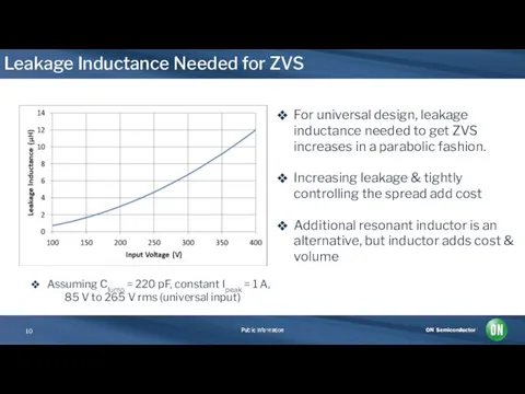
Leakage Inductance Needed for ZVS
For universal design, leakage inductance needed
Leakage Inductance Needed for ZVS
For universal design, leakage inductance needed
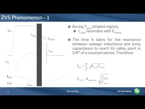
ZVS Phenomenon – 1
During Tdis1 (shaded region),
Lleak resonates with Cclamp.
ZVS Phenomenon – 1
During Tdis1 (shaded region),
Lleak resonates with Cclamp.
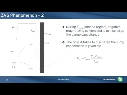
ZVS Phenomenon – 2
During Tdis2 (shaded region), negative magnetizing current starts
ZVS Phenomenon – 2
During Tdis2 (shaded region), negative magnetizing current starts
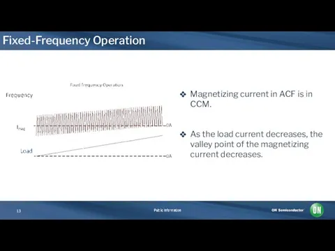
Fixed-Frequency Operation
Magnetizing current in ACF is in CCM.
As the load current
Fixed-Frequency Operation
Magnetizing current in ACF is in CCM.
As the load current
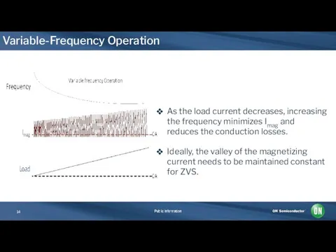
Variable-Frequency Operation
As the load current decreases, increasing the frequency minimizes Imag
Variable-Frequency Operation
As the load current decreases, increasing the frequency minimizes Imag

Light-Load Efficiency
&
Standby Power Challenge
Light-Load Efficiency
&
Standby Power Challenge
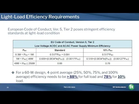
Light-Load Efficiency Requirements
European Code of Conduct, Ver. 5, Tier 2 poses
Light-Load Efficiency Requirements
European Code of Conduct, Ver. 5, Tier 2 poses
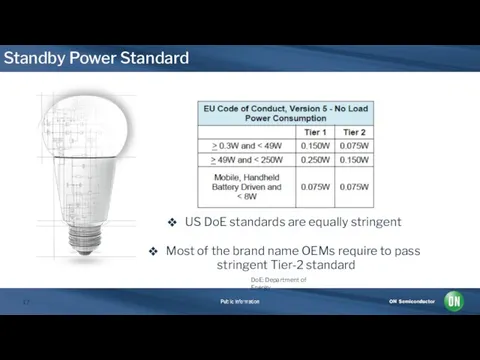
Standby Power Standard
US DoE standards are equally stringent
Most of the brand
Standby Power Standard
US DoE standards are equally stringent
Most of the brand
ACF Specific Light-Load Challenges
Magnetizing current is in CCM.
Frequency modulation results in
ACF Specific Light-Load Challenges
Magnetizing current is in CCM.
Frequency modulation results in
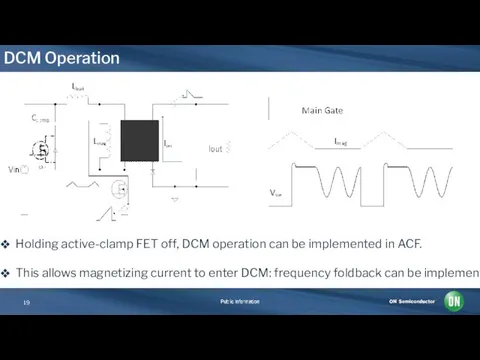
DCM Operation
Holding active-clamp FET off, DCM operation can be implemented in
DCM Operation
Holding active-clamp FET off, DCM operation can be implemented in
Introduction to NCP1568
Ac-Dc PWM Controller for ACF
Introduction to NCP1568
Ac-Dc PWM Controller for ACF
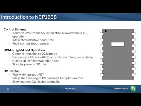
Introduction to NCP1568
Control Scheme
Adaptive ZVS frequency modulation allows variable Vout operation
Integrated
Introduction to NCP1568
Control Scheme
Adaptive ZVS frequency modulation allows variable Vout operation
Integrated
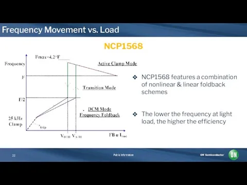
Frequency Movement vs. Load
NCP1568
NCP1568 features a combination of nonlinear & linear
Frequency Movement vs. Load
NCP1568
NCP1568 features a combination of nonlinear & linear
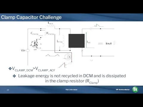
Clamp Capacitor Challenge
VCLAMP_DCM>VCLAMP_ACF
Leakage energy is not recycled in DCM and is
Clamp Capacitor Challenge
VCLAMP_DCM>VCLAMP_ACF
Leakage energy is not recycled in DCM and is
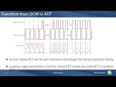
Transition from DCM to ACF
Active-clamp FET can be soft-started to discharge
Transition from DCM to ACF
Active-clamp FET can be soft-started to discharge
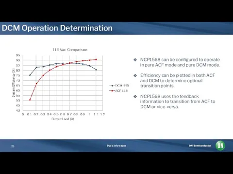
DCM Operation Determination
NCP1568 can be configured to operate in pure ACF
DCM Operation Determination
NCP1568 can be configured to operate in pure ACF

Key Components Selection
Transformer Design & Key Equations
Key Components Selection
Transformer Design & Key Equations
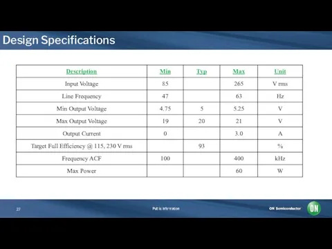
Design Specifications
Design Specifications
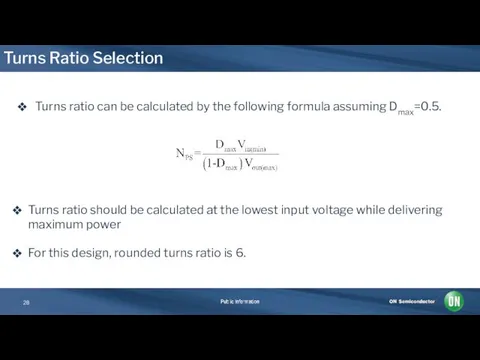
Turns Ratio Selection
Turns ratio can be calculated by the following formula
Turns Ratio Selection
Turns ratio can be calculated by the following formula
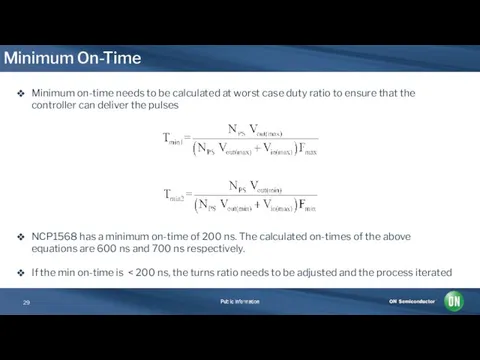
Minimum On-Time
Minimum on-time needs to be calculated at worst case duty
Minimum On-Time
Minimum on-time needs to be calculated at worst case duty
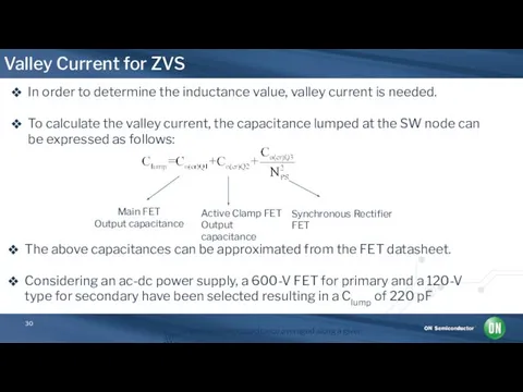
Valley Current for ZVS
In order to determine the inductance value, valley
Valley Current for ZVS
In order to determine the inductance value, valley
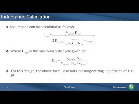
Inductance Calculation
Inductance can be calculated as follows:
Where Dmin is the minimum
Inductance Calculation
Inductance can be calculated as follows:
Where Dmin is the minimum
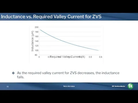
Inductance vs. Required Valley Current for ZVS
As the required valley current
Inductance vs. Required Valley Current for ZVS
As the required valley current
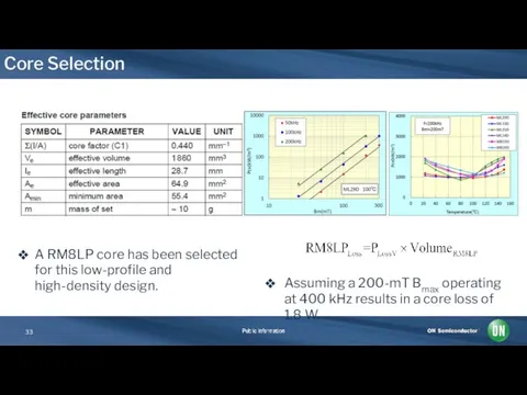
Core Selection
Assuming a 200-mT Bmax operating at 400 kHz results in
Core Selection
Assuming a 200-mT Bmax operating at 400 kHz results in
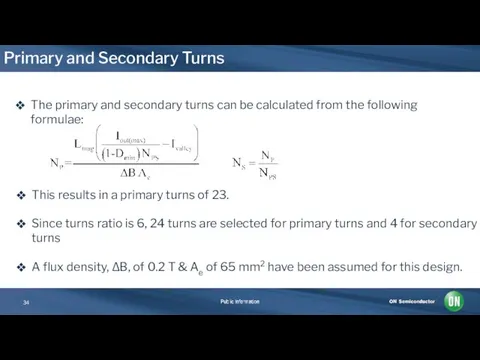
Primary and Secondary Turns
The primary and secondary turns can be calculated
Primary and Secondary Turns
The primary and secondary turns can be calculated
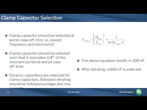
Clamp Capacitor Selection
Clamp capacitor should be selected at worst-case off-time i.e.,
Clamp Capacitor Selection
Clamp capacitor should be selected at worst-case off-time i.e.,
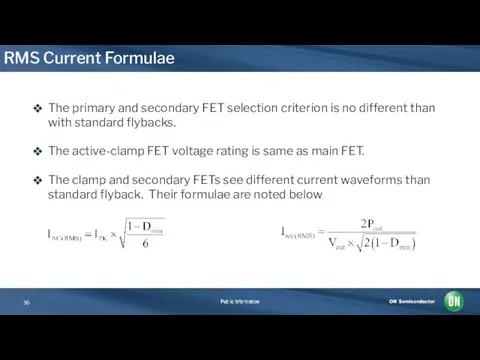
RMS Current Formulae
The primary and secondary FET selection criterion is no
RMS Current Formulae
The primary and secondary FET selection criterion is no
60-W UHD-Board Performance
60-W UHD-Board Performance
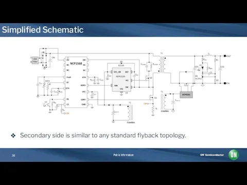
Simplified Schematic
Secondary side is similar to any standard flyback topology.
Simplified Schematic
Secondary side is similar to any standard flyback topology.
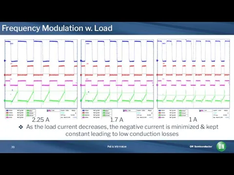
Frequency Modulation w. Load
As the load current decreases, the negative current
Frequency Modulation w. Load
As the load current decreases, the negative current
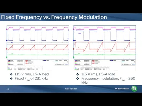
Fixed Frequency vs. Frequency Modulation
115 V rms, 1.5-A load
Fixed Fsw
Fixed Frequency vs. Frequency Modulation
115 V rms, 1.5-A load
Fixed Fsw
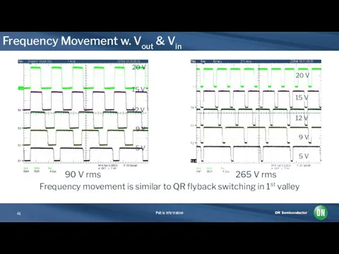
Frequency Movement w. Vout & Vin
Frequency movement is similar to QR
Frequency Movement w. Vout & Vin
Frequency movement is similar to QR
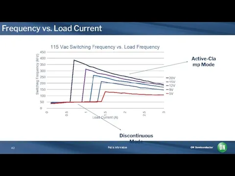
Frequency vs. Load Current
Active-Clamp Mode
Discontinuous Mode
Frequency vs. Load Current
Active-Clamp Mode
Discontinuous Mode
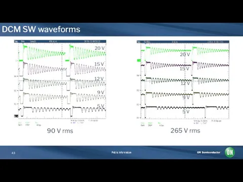
DCM SW waveforms
90 V rms
265 V rms
DCM SW waveforms
90 V rms
265 V rms
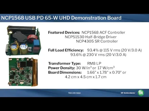
NCP1568 USB PD 65-W UHD Demonstration Board
Featured Devices: NCP1568 ACF Controller
NCP1568 USB PD 65-W UHD Demonstration Board
Featured Devices: NCP1568 ACF Controller
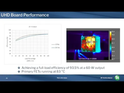
UHD Board Performance
Achieving a full-load efficiency of 93.5% at a 60-W
UHD Board Performance
Achieving a full-load efficiency of 93.5% at a 60-W
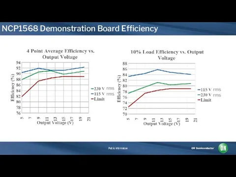
NCP1568 Demonstration Board Efficiency
NCP1568 Demonstration Board Efficiency
 Дестабилизирующие факторы современности
 Щедрость и великодушие 3 класс
 Основные материалы, применяемые в строительстве и их характеристики
 Признаки неблагоприятного СПК и способы его оптимизации (копия)
 Послание к Филимону
 С днём рождения
 20121012_drakon_urok
 Жидкие кристаллы
 Работа с бумагой. Изделие
 Способы толкования слов
 Современные энергосберегающие технологии. Пассивные дома
 Уход за одеждой. Стирка
 Landing gear systems
 Наноматериалы в технологиях механической обработки
 Снаряжение для туризма
 Бумага, ножницы, клей
 pr03
pr03 Кондиціювання мінерального складу води в спосіб Na-катіонування та деаерації
 20120216_kamennye_palatki_na_beregu_ozera_bolshie_allaki
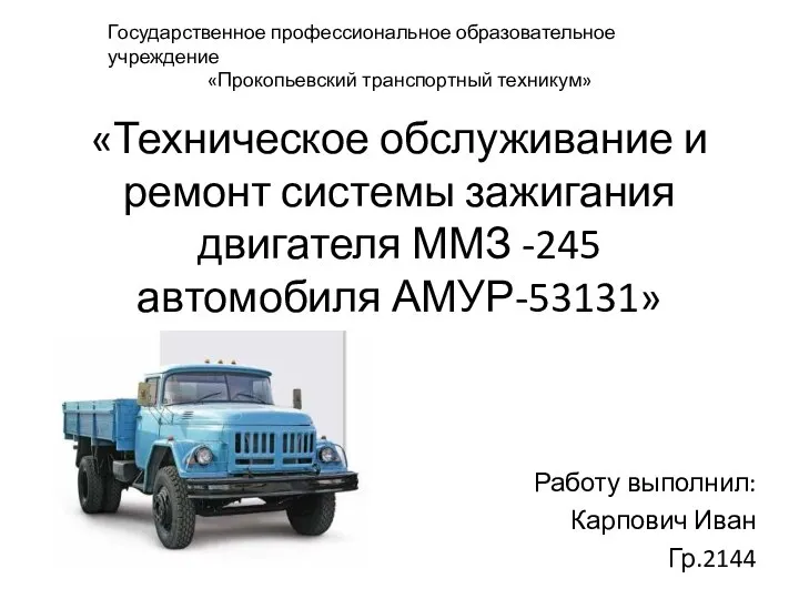 Техническое обслуживание и ремонт системы зажигания двигателя ММЗ -245 автомобиля АМУР-53131
 20160513_fonvizin_d.i._biografiya
 Глава Масло
 Domino. Реконструкция завода и прилегающей территории
 Требования, предьявляемые к убойным животным
 Формирование универсальных учебных действий младших школьников
 Краснодарский_край_презентация_04.08.2022
 Витаминная азбука или зачем нужны витамины
 Қызылорда облысы Ы.Жақаев атындағы күріш шаруашылығы ҒЗИ ЖШС жағдайында минималды технологиямен күріш өсіру технологиясы